
AUGUST 18, 2021 BY ROBERT ASHTON and STEPHEN FAIRBANKS
TLP has become the measurement tool of choice for ESD design engineers exploring circuit properties in the ESD time and current domain. In this introductory post I will first describe the problem that TLP solves and then discuss how TLP is used.
Consider the predicament of a circuit designer tasked with designing ESD protection for an integrated circuit (IC) in a new technology. The starting point for IC design is a knowledge of the properties of the technology. The starting point for most IC designers is the model files that describe the properties of the technology’s transistors, diodes, capacitances, and resistances as well as other parameters of the technology such as breakdown voltages and absolute maximum values specified by the technology developers. This information is insufficient for the ESD protection designer. The available information is perfect for designing an input/output (IO) buffer intended to sense voltages between 0 and 3.3 V or drive 10s of mA continuously. It is not sufficient for human body model (HBM) protection design where the IO needs to sustain an amp of current for about 100 ns, or for the case of charged device model (CDM) where the IO needs to sustain several amps of current for a ns. The situation is even worse if the IO is intended for an external system IO such as USB or HDMI where currents can be 10s of amps and last 60 ns.
The designer needs to know the properties of the technology for currents in the multi amp range but for short times. The normal measurement systems to characterize integrated circuit technologies mostly deal with currents below an amp, and if pulse measurement capability is available the pulse lengths are on the order of many microseconds, not the nanoseconds of an ESD event. Tim Maloney and his co-authors provided what would prove the be the measurement system of choice, transmission line pulse (TLP), in a pair of landmark papers in 1985 [1,2].
A source of multi-amp, short duration pulses can be remarkably simple. A length of co-axial cable, a transmission line, charged to a voltage can produce a multi-amp pulse whose amplitude depends on the charging voltage and the duration depends only on the length of the cable. Implementing this into a usable measurement system is not trivial, explaining why commercial TLP systems are much more expensive than a length of coax cable. The development of this simple pulse source into highly capable measurement systems has proven invaluable for the ESD design community. Other posts in this TLP series will discuss details of TLP systems and measurements. This post will discuss how TLP is used, providing motivation for the following posts in the series.
Figure 1 shows an idealized TLP system. The system consists of a length of coaxial cable which can be charged to a high voltage (HV). An RF relay can disconnect the center conductor from the HV supply and connect it to a coaxial cable leading to the device under test (DUT). A current probe and a voltage probe on the high side of the DUT allow the capture of the current through the DUT and voltage across the DUT by a high-speed oscilloscope. Figure 1 captures the essence of a TLP system. What it lacks is control of reflections, which complicates TLP system design but will be discussed in later posts. This simplified system will provide the necessary background for understanding how TLP systems are used.
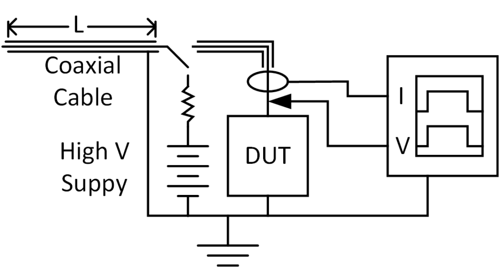
Figure 1 Ideal view of a pulse measurement system for ESD characterization
One of the prime outputs of TLP measurements is a current versus voltage curve (IV) of a circuit element or protection structure in which each IV point is measured during a single TLP pulse. This is explained in Figure 2. A pulse is captured by the digital oscilloscope and the voltage and current are averaged over a measurement time window, usually late in the pulse. Each pulse provides one data point. TLP measurements are usually started with a low charging voltage and after each pulse the charging voltage is increased, mapping out an IV curve as shown in the right half of Figure 2.
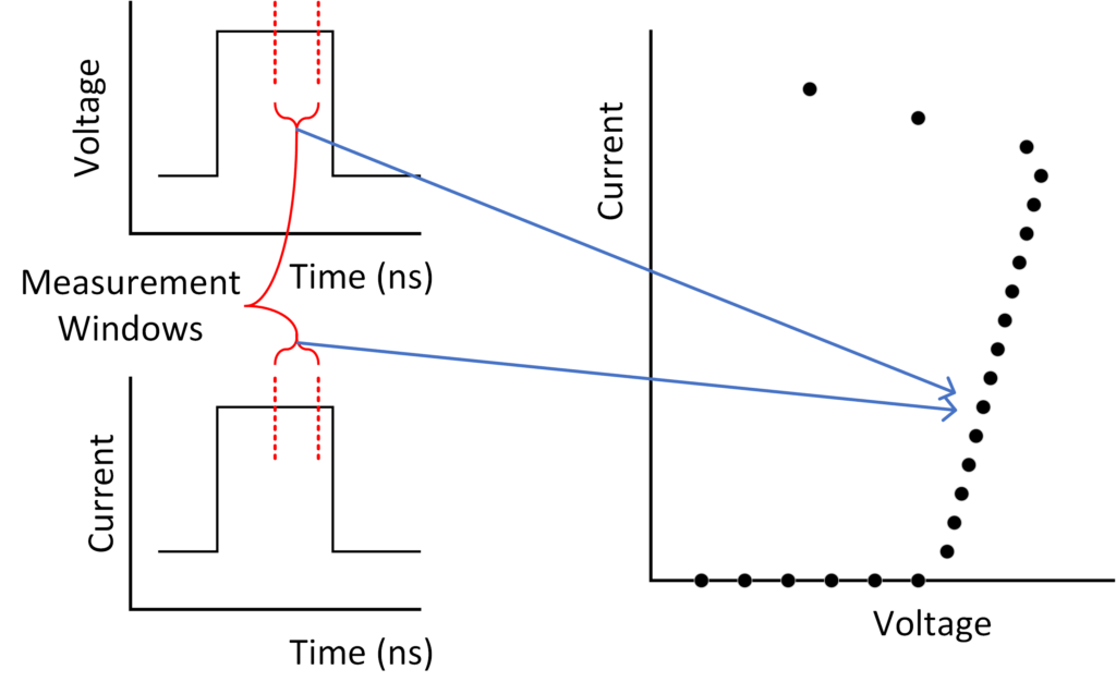
Figure 2 Each TLP pulse is used to create a single I-V point. Repeated pulses, each at a higher charging voltage allows the creation of a full IV curve.
Averaging within a measurement window improves the accuracy of a TLP measurement by removing noise in the measurement. The window is usually chosen late in the pulse for two reasons. TLP systems are high speed measurement systems and unless extreme care is used in their construction there is often ringing or other artifacts near the beginning of the pulse which are not characteristic of the DUT. The initial part of the pulse may also include transient characteristics of the DUT which are best investigated after a good understanding of the quasi-static properties of the DUT.
In the last sentence of the preceding paragraph, I stuck in a word that may have been missed but is especially important, “quasi-static”. TLP IV curves are measured after initial transients, but before significant device heating can occur. This is what sets TLP IV curves apart from what can be measured with traditional current and voltage measurement equipment, device characteristics at high current levels can be determined before significant self-heating.
How much current and voltage a circuit element can survive during an ESD event is crucial information in ESD design. For this reason, most TLP systems include DC leakage measurement circuitry, not shown in Figure 2. After each TLP pulse the system can apply a low DC voltage, usually between 0.5 V and 5 V to look for device degradation. The leakage measurements are often displayed on the same plot as the IV curve using a unique method illustrated in Figure 3. In addition to the standard x axis for voltage and y axis for current a secondary x axis is added for leakage. The leakage measured after each TLP pulse is plotted using the secondary x axis. The y axis position for the leakage measurement is the measured TLP pulse current just proceeding the leakage measurement. This allows the visualization of the development of leakage as the stress current is increased. In the example in Figure 3, leakage is unchanged up to the fourth from the highest current TLP pulse. During the last three pulses the leakage increases after each stress. In this example the increase in leakage is also accompanied by a change in device behavior during the TLP stress. It is not always the case that device damage is accompanied by a change in the TLP IV characteristics.
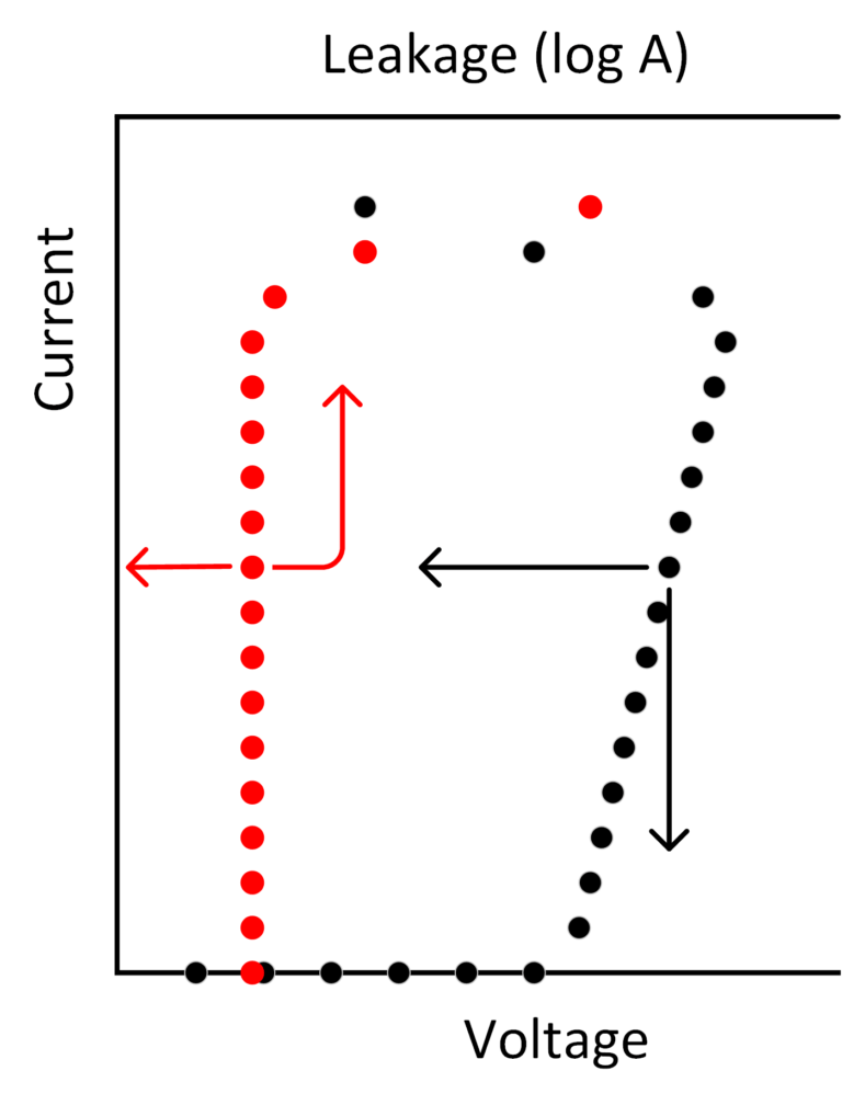
Figure 3 TLP IV curve with accompanying leakage measurements
TLP can also be used to look at time dependence and transients. In its most simple form, the measurement window shown in Figure 2 can be made narrow relative to the width of the pulse and IV curves can be extracted using measurement windows at two or more positions within the pulse.In some TLP systems it is possible to directly measure the voltage and/or current pulses as a function of time to observe phenomena such as turn on time. Most TLP systems include rise time filters so that the effect of rise time during a stress pulse can be determined. This will be discussed in future posts.
TLP is the primary tool of the ESD protection designer for understanding device properties in the ESD range of time and currents. It is also used extensively in failure analysis, both for ESD and EOS issues. The more the measurement technique is understood the better the data from it can be understood and its full potential can be realized. As discussed in the Introduction, future blog posts will go into some of the details of TLP systems and how they can be used.
[1] Maloney, T. and Khurana, N., “Transmission line pulse technique for circuit modeling and ESD phenomena”, EOS/ESD Symposium Proceedings, 1985.
[2] Khurana, N, Maloney T., Yeh, W, “ ESD on CHMOS Devices – Equivalent Circuits, Physical Models and Failure Mechanisms”, 23rd International Reliability Physics Symposium, 1985.
JUNE 10, 2021 BY ROBERT ASHTON and STEPHEN FAIRBANKS
In an earlier blog I discussed the benefits of HBM testing using a low parasitic two pin testing versus a matrix-based tester. In that blog I put off the big challenge of testing with a two-pin tester, setting up the pin combinations to use for HBM qualification testing. In this blog I will tackle that issue. This is a challenge because the widely used JS-001-2017 [1] test standard often assumes a matrix-based tester. What will be shown is that to efficiently do HBM qualification testing of high pin count integrated circuits using a two-pin tester requires a good understanding of the IC to be tested as well as comprehensive knowledge of JS-001 and the various options available to reduce the number of necessary pin combinations.
There are three ways to develop pin combinations for two pin HBM testing, each with a possible option to represent supply pin groups with a single pin.
All of the above options will be covered. As we discuss these options it will become apparent that the more knowledge the test engineer has about the device being tested, the more the number of unique stresses which need to be performed can be reduced.
As with all blogs in this series, this blog is intended to give insight into the HBM test method. There is no substitute for reading the original test method.
Note: In this blog I will often be referring to Table 2A and Table 2B in JS-001. Whenever Table 2A or Table 2B is referenced it is a reference to the JS-001 tables. When Table 1, Table 2, or Table 3 are referenced it is to the tables in this document.
Before discussing pin combinations, the special allowances for package planes and above passivation levels (APL) will be discussed, since these allowances apply to all three methods of developing pin combinations.
JS-001-2017 makes an allowance to represent a supply pin group as a single pin if the supply pin group is tied together by a package plane or an above passivation layer (APL) which connects any two pins in the group with a resistance less than 1 Ohm. A package plane is a metal layer in an IC package tying a number of pins together. An APL is a metal layer on the surface of the die, but above the passivation layer which is used to move the position of various IC connections to more convenient locations for packaging. An APL is often called a redistribution layer.
With the very low resistances of package planes and APL the HBM stress to an IC is really the same if the stress is applied in parallel to all of the pins or to any individual pin of the supply group. Use of the package plane or APL single pin allowance can result in considerable reductions in the number of required pin combinations regardless how pin combinations are being selected.
Note, in HBM testing ground and VSS pin groups are considered supply groups.
In this method every pin is stressed positive and negative against every other pin. Many ESD engineers feel that this is the purest form of HBM testing, since every possible current path is exercised. Others will point out that for higher pin devices this is not allowed, since Section 6.5 of JS-001-2017 states that “Integrated circuits with ten pin or less may be tested with all pin-pair combinations.” It is easy to interpret this statement that if you “may” test all pin combinations if the device is 10 pins or less, you “may not” test all pin combinations if the device has greater than 10 pins. It is my understanding that prohibiting all pin combinations was not the intent and there is likely that this will be clarified in the next release of JS-001. For the rest of this discussion, we will assume that stressing all pin combinations is in fact allowed for all pin count devices.
The challenge of doing all pin combinations is that the number of pin combinations increases rapidly with increasing numbers of pins. Equation 1 calculates the number of unique pin pair combination for an IC with M pins, assuming a low parasitic HBM tester.

Equation 1 takes advantage of the allowance in JS-001 for low parasitic testers that you don’t have to stress pin B versus pin A if pin A versus pin B has been stressed both positive and negative.
Figure 1 shows the number of pin combinations as a function of number of pins if all pin pair combinations are performed. It quickly becomes clear that doing all pin pair combinations for a high pin count integrated circuit (IC) is not reasonable. For low pin count devices stressing all possible pin pair combinations can be a good choice. Assuming 5 seconds to stress a single pin combination positive and negative a 40 pin device could be tested in 65 minutes. While this amount of test time is not short, there is no engineering time expended determining if pins are supply pins, non-supply pins or determining supply pin groupings.
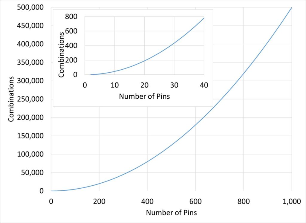
Figure 1 Number of pin combinations for stressing all pin pairs as a function of the number of pins.
JS-001 Table 2B, shown as Table 1 of this blog, is the traditional pin combinations which JS-001 inherited from the legacy JEDEC and ESDA HBM specifications. This method assumes a method of tying a number of pins together, which is most easily accomplished using a matrix based HBM tester. Table 2B includes two types of pin combinations. In combinations 1 through N all pins from a supply pin group are shorted on Terminal B and all pins not on terminal B are stressed, one pin at a time, versus the pins on Terminal B. This is then repeated for each supply pin group. In the second type of pin combinations, N+1, each non-supply pin is stressed versus all other non-supply pins tied together on Terminal B. This is then repeated for each non-supply pin.
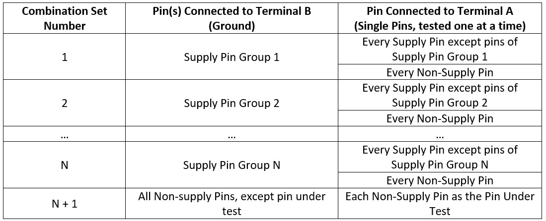
Table 1 Reproduction of JS-001-2017 Table 2B. Notes have been left out.
Performing pin combinations 1 through N+1 on a two pin tester results in a very large number of pin combinations since there is no mechanism for tying Terminal B pins together on a two-pin tester. Each Terminal A pin needs to be stressed to each pin of each supply pin group connected to Terminal B. Considerable relief can be obtained if the pins of each supply pin group are tied together by package planes or APL as will be shown in Section 6.
When performing the N+1 pin combination set on a matrix-based tester there is one pin combination for each non-supply pin. With a two-pin tester it is necessary to stress each non-supply pin to every other non-supply pin individually. In this case the number of pin combinations in pin combination set N+1 is governed by Equation 1 above, where the number of pins, M, would be the number of non-supply pins.
As will be seen in Section 6 it is often unrealistic to perform full HBM qualification testing using a two-pin tester using the traditional Table 2B.
JS-001 Table 2A, shown in Table 2 of this blog, is a more viable option for higher pin count HBM qualification testing using a two-pin tester. Table 2A was first introduced in JS-001-2011 with the goal of reducing test time and reducing failures due to wear out when individual circuit elements were stressed hundreds or thousands of times during HBM testing.
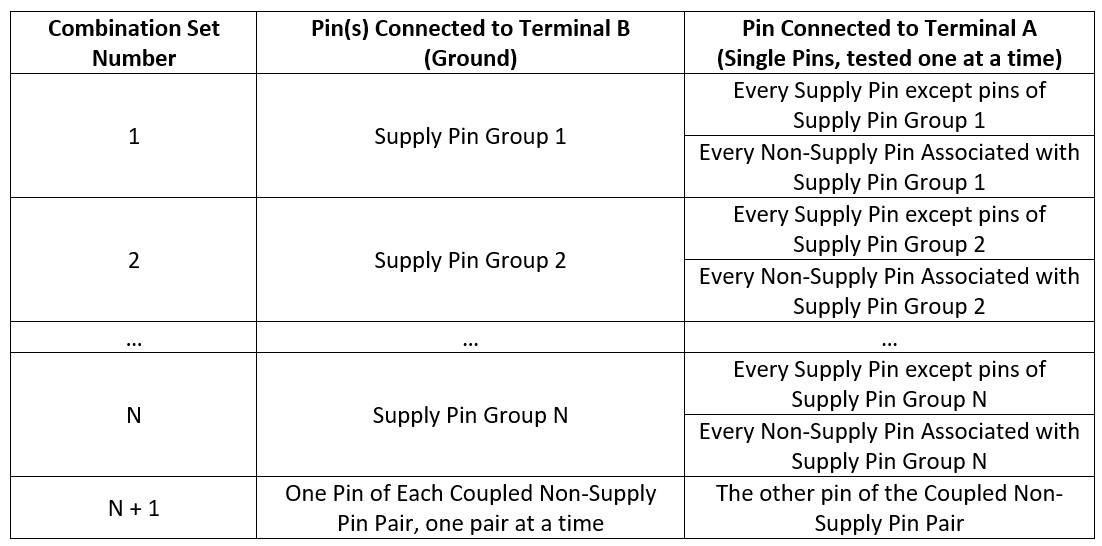
Table 2 Reproduction of JS-001-2017 Table 2A. Notes have been left out.
There are two major changes in Table 2A from Table 2B. One involves the combination sets 1 through N and the second involves combination set N+1.
In both Tables 2A and 2B each supply pin group is tied to Terminal B while pins not in that supply pin group are stressed on Terminal A. In the traditional Table 2B ALL pins not in the Terminal B group are stressed. In Table 2A all supply pins not in the Terminal B group are stressed on Terminal A, but only non-supply pins “associated” with the supply group on Terminal B are stressed. Non-supply pins are associated with a supply if one of two conditions are met:
For ICs with a large number of supply pin groups this can be a significant difference as we will see in the example in Section 6.
In Table 2A Combination Set N+1 there is no longer the requirement to stress each non-supply pin versus every other non-supply pin tied together. This is replaced by a requirement to stress only between “coupled non-supply pin pairs”. A coupled non-supply pin pair is a pair that “may have a potential ESD current path that does not involve supply rails.” The most common example of a coupled non-supply pin pair is a differential input/output pair. If an IC has no coupled non-supply pin pairs there are no pin combinations in set N+1. If there are coupled non-supply pairs there is just one pin combination for each coupled pair. This change significantly reduces the number of pin combinations for ICs with a large number of non-supply pins.
To understand how the different methods of setting pin combinations compare we will consider a specific IC example.
Table 3 lists the number of pin combinations for each of the pin combination options discussed.
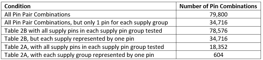
Table 3 Pin combinations necessary to test a 400 pin IC with 8 supply pin groups, 4 VDD groups and 4 VSS groups, with 18 pins per supply pin group. Each non-supply pin is associated with one VDD and one VSS supply group. Half of the non-supply pins are in differential pairs.
If all pin pair combinations are performed there are 79,800 pin combinations. This figure is obtained from Equation 1. If each supply pin group can be represented by a single pin the number of combinations drops to 34,716, as the IC becomes effectively a 264-pin device.
If Table 2B is used and supply pin groups cannot be represented by a single pin there are 78,576 combinations. This is not much of an improvement over doing all pin pairs. The only reduction in pin combinations is that stress between pins in the same supply pin are no longer required.
For Table 2B there is over a factor of two improvement if each supply pin group can be represented by a single pin if the pins are tied together by package planes or APLs. Note that with supply groups represented by a single pin testing all pin pairs and using Table 2B are identical tests. If we assume 5 seconds per pin combination to perform positive and negative stress, 34,716 pin combinations will take over 48 hours for a single device. This level of test time is doable, but is certainly not ideal.
Using Table 2A in a situation where supply pin groups cannot be represented by a single pin yields 13,744 pin combinations. Using the same 5 seconds per pin combination results in a test time of just over 19 hours.
If it is permitted to represent each supply pin domain by a single pin the number of pin combinations drops to a very manageable 604. At 5 seconds per pin combination the test time is just 50 minutes, a very reasonable test time for a single device.
As discussed in a previous blog, testing with a 2 pin, low parasitic HBM tester has considerable advantages in terms of waveform integrity, ability to monitor waveforms and simplicity of current paths during HBM stress. This blog has shown, however, that unless there is a good understanding of the IC being tested and the various options available in JS-001-2017 to reduce the necessary pin combinations test times on a two-pin tester can be unreasonably long and device wear out could become an issue. This is especially true for high pin count ICs with a large number of supply groups.
It is important to remember, that even if the number of pin combinations becomes too large to allow a two-pin tester to be used for HBM qualification, the two-pin tester remains unparalleled for diagnostics.
[1] “For Electrostatic Discharge Sensitivity Testing Human Body Model (HBM) – Component Level”, ANSI/ESDA/JEDEC JS-001-2017.
JANUARY 14, 2021 BY ROBERT ASHTON and STEPHEN FAIRBANKS
This post will be discussing the differences between the ESD qualification requirements for integrated circuits intended for standard commercial applications and for automotive applications. Automobiles have always had electrical circuits. Even before electric headlights and electric starters, magnetos provided electrical pulses to power spark plugs. The amount of electrical circuitry increased steadily over the years, and today the radio was replaced long ago as the most sophisticated piece of electronics in a vehicle. The rapid expansion in the high-tech electronic content in the automobiles has attracted increased interest across a much wider section of the electronics industry than it has in the past. Integrated circuit suppliers wishing to become suppliers to the automotive industry must become familiar with the qualification requirements for automotive electronics.
The working environment for automotive electronics is much more severe than is common for most consumer applications. Automotive electronics must work in the dead of winter in Minnesota and crossing Death Valley in the summer. The automotive environment is also an electrically noisy environment, with wiring harnesses carrying sensing circuits as well as high current pulses to operate a wide range of motors and accessories. Automotive electronics are also often safety critical. It is therefore not surprising that the automotive industry has their own set of qualification requirements for electronic components.
Note: In this post I am trying to summarize the differences between ESD qualification for commercial and automotive integrated circuits. This summary should not be used as a substitute for a thorough reading of the full standards.
The qualification requirements for most commercial integrated circuits are dictated by JEDEC’s JESD47 “Stress-Test-Driven Qualification of Integrated Circuits” [1], while automotive integrated circuits are specified by the AEC (Automotive Electronics Council) Q100 standard, “Failure Mechanism Based Stress Test Qualification for Integrated Circuits” [2]. These two documents are very similar in their purpose and methodology. The two documents include the following types of requirements.
A list of stress tests required for qualification such as:
Specification of the test method to be used for each test
Specification of requirements for each test such as:
When each of the tests are required such as:
We can now compare the requirements for ESD testing in the JEDEC and AEC qualification documents. To do this the table entries for HBM and CDM in the two documents will be reproduced here, eliminating two columns from the AEC table which are not relevant to the current discussion.

Table 1 JEDEC requirements for HBM and CDM in JESD47K

Table 2 AEC requirements for HBM and CDM in Q100H
There are three notable differences between the qualification requirements in the two methods.
The difference in the test standards is not as stark as it seems. At the beginning of the AEC Q100-002 for HBM and Q100-011 for CDM are the following statements respectively.
All HBM testing performed on Integrated Circuit Devices to be AEC Q100 qualified shall be compliant to the latest revision of the ANSI/ESDA/JEDEC JS-001 specification, with additional requirements as defined herein.
All CDM ESD testing performed on Integrated Circuit devices to be AEC Q100 qualified shall be per the latest version of the ANSI/ESDA/JEDEC JS-002 specification with the following clarifications and requirements.
These statements show that the basic tests for HBM and CDM are essentially the same between JEDEC and AEC. The number of samples required is also the same. While JESD47 specifies three samples, JS-001 also specifies three samples. Q100-002 for HBM does not specify the number of samples, so the AEC requirement is governed by the three samples required by JS-001. For CDM, Q100-011 specifies three samples.
The difference in requirements is more substantial. JEDEC lists the requirements as “Classification”. The requirement is therefore that all integrated circuit designs must be tested for both HBM and CDM. The actual requirement is set by agreement between the manufacturer of the integrated circuit and the purchaser. For many years it was “common knowledge” that the specification for HBM was 2000 V and that that requirement was being reduced to 1000 V due to the activity of the Industry Council on ESD Targets. This “common knowledge” was in fact never true, for commercial product the ESD levels for both HBM and CDM have always been an agreement between supplier and purchaser.
AEC is much stricter in terms of requirements for HBM and CDM. The basic benchmarks for AEC ESD are an HBM passing level of 2000 V and a CMD passing level of 750 V for corner pins and 500 V for all other pins. As can be seen in Table 2, there are exceptions. Lower levels of ESD robustness can be accepted by the user. The note to see Section 1.3.1 is a requirement for reporting which reads:
For ESD, it is highly recommended that the passing voltage be specified in the supplier datasheet with a footnote on any pin exceptions. This will allow suppliers to state, e.g., “AEC-Q100 qualified to ESD Classification 2”.
Most of the remaining differences between the JEDEC and AEC ESD requirements are in the additional requirement in Q100-002 for HBM and Q100-011 for CDM.
This section will summarize the additional requirements for HBM testing according to Q100-002.
This requires that all the tester meeting the waveform requirements at all test levels. (Legacy wording in JS-001 could be interpreted that the tester didn’t need to meet all waveform requirements, but this was never the intension.)
Requires test fixture board meet waveform requirements at all test voltages, not limited voltages. Also specifies requalification if the board is repaired.
Requires that device stressing be done at 500 V, 1000 V and 2000 V. Levels may not be skipped. JS-001 allows testing at a single level to establish the immunity level. Q100-002 also specifies that if the device fails 500 V, it requires testing at 250 V, and if that fails testing at 125 V if the tester can meet the waveforms.
Devices with 6 pins or less must be tested with all pin pair combinations. (One pin on Terminal A and one pin on Terminal B.) JS-001 requires that discrete devices be tested with all pin combinations and allows devices with 10 or less pins to be tested with all pin pair combinations.
JS-001 includes two options for pin combinations. Table 2B is the traditional pin combinations from the original version of JS-001 and is the same set of pin combinations as in the now obsolete HBM standards from JEDEC and ESDA. Table 2A is a new table which reduces the number of stresses on an integrated circuit, but requires more understanding of the device under test. The purpose of Table 2A is to reduce test time and, possibly more important, to reduce failures due to wear out. Q100-002 requires all testing to start using Table 2B.
Q100-002 requires the use of Table 2B, but does give three options in which Table 2A may be used.
Q100-002 has special instructions if using a low parasitic tester such as a two-pin tester.
Q100-002 has a section on reporting, which is lacking in JS-001. In addition to reporting the basic test results the reporting section requires information on the type of tester used, details on the samples and test details such as pin groupings, stress voltage levels, any portioning of stress over multiple devices, stress pin combinations, and any exceptions for the tests performed.
This section will describe the additional testing requirements for CDM testing according to Q100-011
250 V is a required test level, and if higher withstand levels are to be reported testing has to be done in 250 V increments up to the highest passing level. It is not permissible to skip stress levels. If a device fails at 250 V testing is to be done at 125 V and if failure occurs at that level lower levels such as 100 V and 50 V are to be used. JS-002 allows testing at a single voltage and if all requirements are met that level can be used as the devices CDM withstand level.
One of the most significant differences between JS-002 and Q100-011 is the number of zaps to each pin per voltage and polarity. Q100-011 requires 3 stresses on each pin for each voltage and polarity, while JS-002 requires “at least 1 discharge” per voltage and polarity. The wording of “at least 1 discharge” was added to JS-002 so that a single set of testing could cover both JS-002 and AEC Q100-11 testing.
A unique feature of the AEC CDM is the corner pin requirement. As discussed in Section 2 the standard qualification level for CDM is 500 V, with corner pins at 750 V. Section 1.3.1 of AEC Q100-11 describes the definition of a corner pin, while Section 2.7 describes two methods to determine the 750 V corner pin classification.
This section of Q100-11 discusses the difficulties of CDM testing of small package, and notes that in some cases it the testing may need to be skipped, but this must be noted and done in agreement with the user. This section came out before JS-002 included provisions to eliminate further CDM testing of small devices within a technology family with a known CDM history of robustness.
This section discusses CDM testing of products shipped at wafer level or as bare die. The document allows bare die product to be tested in a surrogate package, as long as the package used is documented.
This section defines failure as not meeting all device specifications. The section also notes that after CDM testing device parameters can drift from out of specification back into specification. This section encourages post stress testing to be done soon after stress, but does not give a time limit.
This section requires that to pass a specified classification level the device must also pass all lower test levels.
There are also some slight differences in the classification levels between JS-002 and Q100-11. To account for the 750 V corner pin requirement, AEC has inserted an extra level into their classification scheme, creating some confusion. The new Q100-11 level of C2 has the same definition as the JS-002 definition as JS-002 level C2a. To obtain the C2a level in Q100-11 requires corner pins passing 750 V or higher.

Table 3 Comparisons of JS-002 and Q100-11 qualification levels
In summary, the ESD requirements for commercial versus automotive qualification are very similar. Both require HBM and CDM testing based on the same two test standards, JS-001 for HBM and JS-002 for CDM. Automotive qualification has additional requirements, including specified qualification target levels, 3 versus 1 zap for CDM, and a number of additional requirements. The good news is that if a product has met the requirements of AEC Q100 for ESD qualification, the product will more than met the requirements for JEDEC/ESDA qualification for ESD.
[1] JESD47, “Stress-Test-Driven Qualification of Integrated Circuits”, JEDEC Solid State Technology Association, https://www.jedec.org/.
[2] AEC – Q100 – Rev-H, “Failure Mechanism Based Stress Test Qualification for Integrated Circuits” Automotive Electronics Council, http://www.aecouncil.com/.
[3] ANSI/ESDA/JEDEC JS-001-2017, “For Electrostatic Discharge Sensitivity Testing, Human Body Model (HBM) – Component Level”, EOS/ESD Association, https://www.esda.org/, and JEDEC Solid State Technology Association, https://www.jedec.org/.
[4] ANSI/ESDA/JEDEC JS-002-2018, “For Electrostatic Discharge Sensitivity Testing, Charged Device Model (CDM) – Device Level”, EOS/ESD Association, https://www.esda.org/, and JEDEC Solid State Technology Association, https://www.jedec.org/.
[5] AEC–Q100-002 REV-E, “Human Body Model Electrostatic Discharge Test”, Automotive Electronics Council, http://www.aecouncil.com/.
[6] AEC-Q100-011 Rev-D, “Charged Device Model (CDM) Electostatic Discharge (ESD) Test”, Automotive Electronics Council, http://www.aecouncil.com/.
OCTOBER 19, 2020 BY ROBERT ASHTON and STEPHEN FAIRBANKS
This blog will discuss the differences and advantages of two popular types of Human Body Model (HBM) testers for evaluating electronic components for ESD robustness, two pin and matrix based testers. In a future blog I will discuss setting up pin combinations with a two pin tester.
HBM [1] is the most popular electrostatic discharge (ESD) test method for electronic components such as integrated circuits, transistors, diodes and other electronic components to ensure that they have sufficient ESD robustness to survive in an ESD controlled manufacturing environment. In earlier blogs I have discussed the HBM current waveform, tester parasitics, and pin combinations. If you are not familiar with those topics, a quick read of those blogs would be very helpful in understanding the comparison of two pin and matrix-based testing.
The title of this blog, Two Pin Versus Matrix HBM Testing, could be misinterpreted. In this article two pin refers to a tester which has only two pins or terminals, a stress terminal (Terminal A) and a return terminal (Terminal B). It could also be interpreted as testing one pin versus a single other pin. Within the HBM field, and in this article, that type of testing is referred to as pin pair testing. To avoid this confusion, we will first define the terms that will be used in this blog, and then expand upon the definitions and discuss the advantages and disadvantages of the two types of testers.
These definitions are for the purpose of this blog and are not “official” JS-001 HBM standards definitions. It is also good to note that in HBM testing Terminal B is often referred to as ground. In most cases that is not strictly true. HBM tester often have a resistance in the range of 50 to 100 ohms between Terminal B and true system ground to prevent reflections.
Pin pair testing is probably the “purest” form of HBM testing. If all possible paths between pins were covered with pin pair testing any weak paths would be discovered. It would also seem to be the easiest to perform diagnostics on if there is a failure. All current enters one pin and exits through another single pin.
In the earliest days of HBM testing all testing was probably two pin testing. As the number of device pins increased a major limitation soon emerged with regard to two pin testing, doing all possible pin combinations takes a long time.
One of the solutions to the long time that two pin testing takes is ganged pin testing. Rather than performing all pin combinations, a single pin on Terminal A could be stressed versus a number of similar pins on Terminal B. This led to the traditional pin combinations in Table 2B of JS-001 [1]. Single pins are stressed on Terminal A, versus pins shorted (ganged) together on Terminal B. Rather than stressing a single pin versus every power and ground pin individually, groups of power and ground pins connected together in the package or on the die are also shorted together in the tester. To find possible weak links between non power pins, each Input or Output pin was stressed to all other Input and Output pins tied together. This method significantly reduced the number of stressed to a device and improved test time considerably. With this type of testing the actual current path of each stress is less well defined.
Two pin testers are both the oldest and newest type of HBM tester. A two pin tester can only perform pin pair testing. The very earliest HBM testers were probably two pin testers, a power supply, an RC(L) network, a switch and probably clip leads to the DUT. Two pin testers have never truly gone away, and can be very useful for low pin count devices. The ETS 910 existed for many years, and its replacement the ETS 9910, are essentially two pin testers, using a pair of short leads to connect the pulse source to the DUT.
The newest breed of two pin testers is represented by the Grund Technical Solutions Pure Pulse HBM system. Rather than clip leads, the Pure Pulse system uses RF wafer probers to connect to the device under test, as shown in Figure 1. The wafer probers, with 50 ohm impedance to within millimeters of the DUT, ensure that the waveform is delivered to the DUT with minimal distortion and vanishingly low parasitics. The Grund system can also accurately measure the current through the DUT and voltage across the DUT on each HBM pulse. This can be very helpful in diagnosing device functionality and any transformation to a damaged state. [2] The use of robotic wafer probers with the Pure Pulse system facilitates fully automated HBM testing for both packages and at wafer level. The Grund Pure Pulse system is heavily used by Minotaur Labs for both HBM and transmission line pulse (TLP) testing.
Figure 1 Wafer probers from a Pure Pulse HBM system contacting a ball grid array package
In manual HBM testers the DUT is placed in a socket. Jumpers or specialized pins can be used to connect a single, or multiple pins to Terminal B, while a jumper or other connection is used to connect Terminal A to a single pin. These systems can be useful for low pin count devices, especially in a laboratory only doing occasional HBM testing. A classic example is the IMCS 700, later manufactured by Oryx as the M700. Grund Technical Solutions’ Titan ESD tester is a recent addition to the manual tester environment.
The high pin counts on modern integrated circuits and the lager number of pin combinations called out by the HBM standards, even with pin ganging, suggests the need for automation. The relay matrix based HBM tester is the logical evolution of this need. A matrix of relays allows any single pin of a DUT inserted into the tester’s socket to be connected to Terminal A and one or more pins to be connected to Terminal B. The use of a relay matrix to complete the A and B connections allows for fully automated testing. The Thermo Fisher MK1, MK2 and MK4 family of testers is one of the most widely used examples of relay matrix based HBM testers. Minotaur Labs performs its relay matrix based testing on an MK2.
In a previous blog post I discussed in some detail the issue with tester parasitics, but I will review here. There have been a number of reports that tester parasitics can cause false failures in matrix based HBM testers [3, 4) and the problem was studied in detail by Chaine et al. [5]. Figure 2 shows a schematic that explains how parasitics in an HBM tester can change waveform properties. Many high pin count devices have multiple pins shorted together for power or ground. In a relay matrix based tester, unless a special test fixture is used, each of these pins will be connected to a channel on the matrix. Even if the relay to a pin is not closed, the relay has capacitance across its terminals. This can distort waveforms as shown in the simulated waveforms in Figure 3. The waveform that exits the DUT pin, IT-B, differs considerably from the injected HBM waveform, IT-A, due to the transient currents to the parasitic capacitors, IPAR. Note that the issue with tester parasitics does not just depend on parasitics on the Terminal B side. Tester channels tied together on the A side can also modify waveforms. Inputs and Outputs are also affected. Stress to an IO will often forward bias diodes to power or ground. If the power or ground group has multiple pins the tester parasitics can distort waveforms in this case also. This was shown in [4].
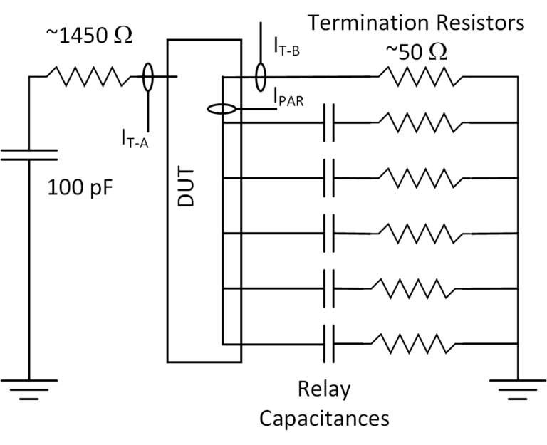
Figure 2 Schematic to explain tester parasitics.
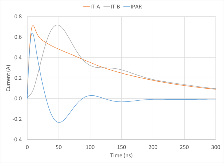
Figure 3 Terminal A, Terminal B, and Parasitic Current in a simulation with 32 channels tied together in the package.
The goal of HBM testing following the JS-001 test standard is to get a reliable, repeatable and reproducible measure of the robustness of an integrated circuit during manual handling in an ESD controlled environment. It is also desirable to have a well-defined current path for easy diagnosis when failure levels are below expectation. These goals are easiest to obtain with pin pair testing with a low parasitic HBM tester.
Pin pair testing can be done with any HBM testers. With a matrix based tester the stress waveforms can differ substantially from the intended HBM waveform, as discussed in the section on tester parasitics. With pin pair testing on a matrix based tester it is true that all current enters by a single pin and eventually exits by a single pin. The current paths between those two pins can be very complex in a matrix based testers, since all pins have parasitic capacitances connected to them. Currents can flow out of, and then back into the DUT as parasitic capacitances charge and then discharge. In recent years some manufacturers of matrix based testers have redesigned the testers to reduce parasitic capacitances. This allows the Terminal B current waveform to stay in specification with higher numbers of pins tied together by the device under test, as well as reducing currents in pins not directly tied to Terminal A or Terminal B. However, for larger pin count devices, with more pins tied together in the package, Terminal B waveforms will still go out of specification and current paths within the device under test will still be hard to understand.
Pin pair testing can also be done on manual HBM testers. In many cases manual tester can be considered “true” low parasitic HBM testers. Manual testers, with their generally low pin counts, typically have large spacings between the traces leading to different pins, resulting in very low capacitance between different pins.
We have found pin pair testing with the Grund Pure Pulse HBM system to be the most straight forward method for performing pin pair HBM testing. The inherently low parasitic nature of the system ensures repeatable, in specification, waveforms and the robotic wafer probers allow automated testing at both package and wafer level. The Grund tester also allows waveform capture during each pulse, which can be very useful during failure analysis. [2]
In short, YES! Matrix based testers have, and will continue to serve the electronics industry well. They have uncovered untold numbers of designs that were weak for HBM robustness. Using JS-001 pin combinations in either Table 2A or 2B, matrix based testers can perform HBM testing in an efficient and thorough manner. There have, however, been multiple instances that the parasitics that distort HBM waveforms have caused false failures. These false failures have consumed considerable resources in time and engineering effort. On the other hand, I know of no instances of a worse problem, false passes that have led to high yield loss due to a device with weak HBM levels getting into high volume manufacturing.
Pin pair HBM testing with an automated two pin tester, with voltage and current capture on each pulse provides the cleanest waveforms, easy to understand current paths and built in diagnostics. Matrix based HBM testing will, however, continue to be a valuable tool in the electronics industry for many years to come. Manual HBM testers are also a valuable tool for low pin count devices and in test laboratories with a low volume of HBM testing. In a future blog I will discuss setting up the pin combinations using a two pin tester, such as the Grund Pure Pulse system.
[1] ANSI/ESDA/JEDEC JS-001-2017, For Electrostatic Discharge Sensitivity Testing Human Body Model (HBM) – Component Level
[2] ROBERT ASHTON and STEPHEN FAIRBANKS, Stephen Fairbanks, Adam Bergen, and Evan Grund, “Electrostatic test structures for transmission line pulse and human body model testing at wafer level”, 2018 IEEE International Conference on Microelectronic Test Structures (ICMTS).
[3] W Anderson, et.al. “Cross-Referenced ESD Protection for Power Supplies”, EOS/ESD Symposium, 1998.
[4] H. Kunz, R. Steinhoff, C. Duvvury, G. Boselli, and L. Ting, “The Effect of High Pin-Count ESD Tester Parasitics on Transiently Triggered ESD Clamps”, EOS/ESD Symposium, 2004.
[5] M. Chaine et.al., “HBM Tester Parasitic Effects on High Pin Count Devices with Multiple Power and Ground Pins”, EOS/ESD Symposium, 2006.
JUNE 5, 2020 BY ROBERT ASHTON and STEPHEN FAIRBANKS
For the ESD test engineer one of the most frustrating challenges is charged device model (CDM) testing very small integrated circuits. During field induced CDM testing, following the joint JEDEC/ESDA CDM standard JS-002 [1] the device under test (DUT) is placed “dead bug” position on the field plate, as shown in Figure 1. The DUT is held in place by vacuum through a small hole in the field plate. For large devices, with flat tops, this method works well. As will be discussed below, this does not work well with small devices, and testing can be an exercise in frustration. Heightening the frustration is that the small devices almost never fail CDM, leaving the test and product engineers wondering why are we going through all this hassle. In this blog I will review some of the challenges of testing small devices, discuss why testing of small devices still should be done, note some of the ways test engineers have addressed the problems, and discuss changes to the latest version of JS-002 which can reduce the amount of CDM testing of small devices.
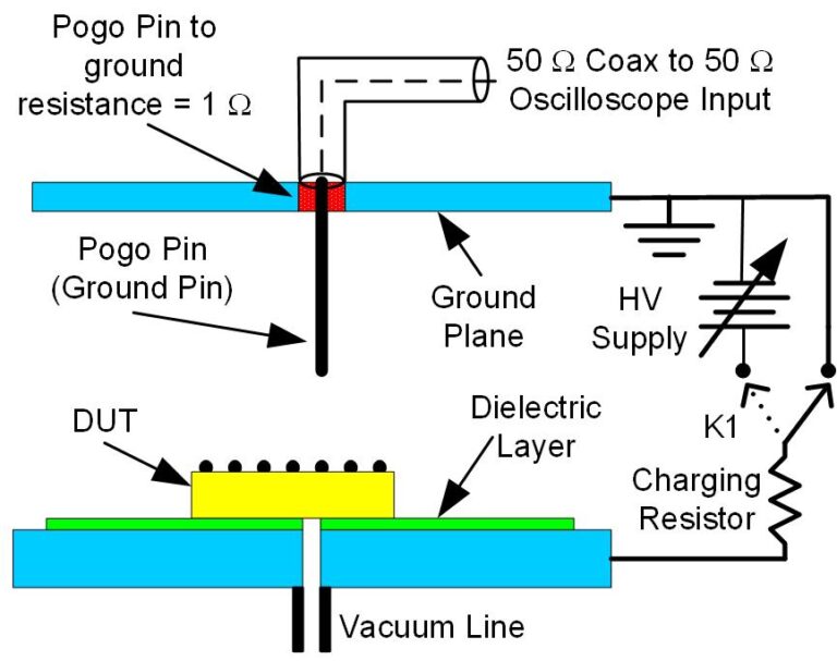
Figure 1: Cross section of a field induced CDM tester showing the vacuum hole to hold the DUT in place
Small devices, with very small area, will have a very small vacuum hold down force, while the force of the pogo pin when it touches the DUT will not change with DUT size. The result for a small ball grid array (BGA) package, if the pogo pin does not touch a ball in the exact center the DUT is pushed to the side and subsequent pogo pin approaches will be misaligned. The problem is more difficult for some classic package types such as SOT-23 (small outline transistor) packages. Figure 2 illustrates how the pogo pin touching the pins of a SOT package will have considerable leverage, making if very likely to dislodge the DUT during testing.
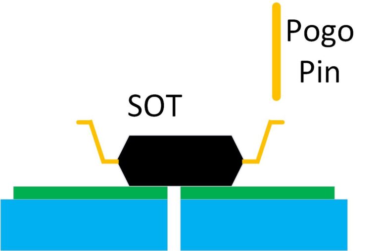
Figure 2 CDM testing of a SOT package
Additionally, JS-002 requires that the area of the DUT be at least 4 times the area of the vacuum hole. If this requirement is not met, the DUT must be placed away from the vacuum hole. Other means of supporting the DUT must then be used.
A variety of techniques have been used to stabilize packages during CDM testing. [2] One of the most popular is to use some kind of physical support, such as a hole cut in thin FR-4 to anchor the package in place, as illustrated in Figure 3. This method can be effective, but it is a challenge to create the cutout in the FR-4. Too large an opening and the DUT will not be well supported. Too small an opening and the DUT will not sit flush with the Field Plate surface, resulting in an invalid CDM test.
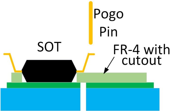
Figure 3 SOT package being supported by an FR-4 template during CDM testing.
Figure 3
Another method that is popular with very small devices, such as chip scale packages, is the use of a conversion board. The conversion board is a small circuit board designed specifically for the DUT to be tested. The conversion board serves to make the tiny package mimic an easy to test package such as a dual inline package (DIP). The use of a conversion board makes the actual CDM testing very easy, but there are two disadvantages. First of all is the considerable time and effort of designing and building the conversion board. Secondly, how well does the DUT, mounted on the conversion board, represent the true CDM characteristics of the DUT. It is often the case that the capacitance between the Field Plate and the DUT plus conversion board is considerably greater than the capacitance of what the DUT to Field Plate would be. This can result in a more severe CDM test than if CDM could be conducted on the DUT alone. An addition change in the CDM test behavior is the conversion board will add considerable inductance to the stress path, changing the characteristics of the CDM stress. With those caveats, it is useful to note that I don’t know of any instances in which the use of a conversion board during CDM testing yielded such erroneous results that it led to field failures due to CDM weakness.
Experience has shown that small devices very seldom, if ever, fail CDM testing. This makes technical sense. In a previous blog post, “CDM Dependence on Device Capacitance”, I discussed how the amount of charge in the CDM pulse gets very small for extremely small devices. This leads inevitably to the question, why CDM test small devices? That same blog post also points out that as the DUT capacitance gets very small, the CDM pulse width gets very narrow. The result is that the peak CDM current does not become vanishingly small, and peak current is often considered the cause of CDM failures.
The joint JEDEC/ESDA CDM working group, which maintains the JS-002 CDM test method, formed a task group, which I led, to consider placing a lower limit on package size for CDM testing. After considerable discussion and consideration of the continuing shrinking of feature sizes in integrated circuit, none of the members of the task group were able to defend a specific size or capacitance below which CDM testing is no longer needed. The task group did define a procedure to allow CDM testing to be eliminated for devices with a DUT to Field Plate capacitance below a technology dependent CSMALL value, if a set of strict criteria are met. This procedure will be discussed in the next section.
In the latest version of the joint JEDEC/ESDA CDM standard, JS-002, [1], there is a new option that can be used to reduce testing of small packages. The new procedure only applies to groups of products made in the same technology. The same technology includes the following:
If the following procedure is followed it is possible to eliminate CDM testing for devices with DUT to Field Plate capacitance less than an experimentally determined CSMALL for the technology. CSMALL for the technology is determined with the following procedure.
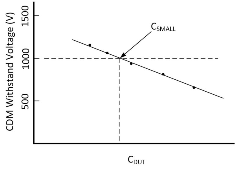
Figure 4 CDM withstand voltage versus CDUT to determine CSMALL
Once CSMALL has been determined, further devices in that technology need not be tested if they meet all the requirements for being included in the technology and the device has been tested and passed the HBM requirements for the technology. Devices that have not been CDM tested based on the above criteria are assigned a CDM withstand level of 750 V. Note: the requirement for doing HBM testing is not because there is a correlation between CDM robustness and HBM robustness. It is simply to ensure that ESD protection elements have been included in the design.
CDM testing of very small integrated circuits can be challenging, because the small size makes them difficult to hold in place using the traditional vacuum hole method. Methods to improve the testability of small devices include the use of FR-4 templates to hold the DUT in place and mounting the DUT on a conversion board to simplify device handling. While most small devices have very high CDM robustness levels, it is not possible to eliminate testing all together because peak current during a CDM test remains high, even for very small packages. Recent changes to JS-002 have allowed elimination CDM of testing of small devices within a device technology if the device’s CDUT is less than the experimentally determined CSMALL for the technology.
MARCH 2, 2020 BY ROBERT ASHTON and STEPHEN FAIRBANKS
In a previous blog “Field Induced CDM Explained” I discussed what happens during the CDM test. This included the sequence of events as voltage is applied to the field plate, how the potential on the device under test (DUT) tracks the field plate, and how the DUT actually becomes charged when the pogo pin “discharges” the DUT. The difference between single pulse and dual pulse test sequences was also explained. This blog will focus on what happens during the CDM pulse itself, and will show how the pulse properties change as a function of DUT to Field Plate capacitance. If you are unfamiliar with how the DUT potential is controlled by field induction during CDM testing it is suggested to read the earlier blog, “Field Induced CDM Explained” first. In this discussion we will start from the situation in which the Field Plate is at an elevated voltage and the DUT has a potential close to the Field Plate potential.
We will see several CDM properties in this blog:
Figure 1 shows a diagram of a field induced CDM (FICDM) tester on the left and an equivalent circuit superimposed on the right. This three-capacitor model for the CDM tester was discussed by Montoya and Maloney [1] and will be used in the present discussion. A more advanced, 5 capacitor model was introduced by Atwood et all in 2007. [2] The 5-capacitor model includes capacitance to the tester chassis and helps explain waveshape after the main pulse. The 5-capacitor model was a significant contribution to understanding of CDM, but is not needed for the current discussion. We will, however, use the capacitance values as determined by Atwood as well as his arc resistance value in the discussion.
The three capacitors in the 3-capacitor model are CDUT, the capacitance between the DUT and the Field Plate, CDG, the capacitance between the DUT and the Ground Plane, and CFG, the capacitance between the Field Plate and the Ground Plane. All three of these capacitances change as the size of the DUT varies.
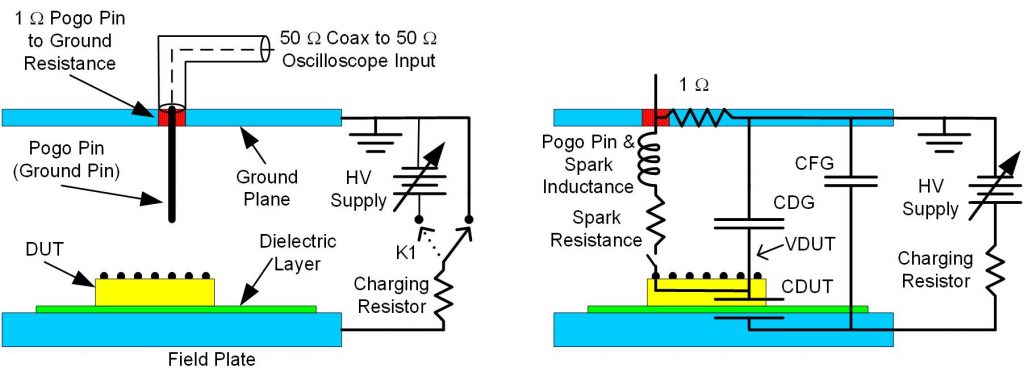
Figure 1 Field Induced CDM tester and equivalent circuit
The easiest capacitance to understand is CDUT, since it is primarily a parallel plate capacitor. In the simulations presented here, with one exception, the DUT is a round coin module, similar to that used as the calibration module in the JS-002 CDM test standard [4]. In a real integrated circuit, the DUT capacitance would be the integrated circuit die’s capacitance to the field plate as well as the capacitance of all interconnect traces or lead frame to the field plate. As the physical size of the DUT increases CDUT will increase. At larger sizes CDUT will be roughly proportional to the DUT area. At small sizes, however, CDUT does not approach zero, since at the smallest sizes fringing field capacitance will dominate.
Similarly, as DUT size increases CDG will increase. At large sizes CDG will always be considerably less than CDUT because the length of the pogo pin is always much larger than the thickness of the Field Plate dielectric. For very small DUT sizes CDG will reach a minimum value, because the DUT to pogo pin capacitance at the time of the CDM arc creates a lower limit for CDG.
CFG also changes in magnitude as the DUT size varies. As the DUT gets larger it creates a shield between the Field Plate and Ground Plane, reducing CFG. In the limiting case where the DUT size is larger than the 2.5 inch (63.5 mm) square ground plane direct field lines between the Field Plate and the Ground Plane will be largely blocked.
To gain insight into the CDM behavior, the circuit in Figure 1 was simulated in LTSpice and the circuit is shown in Figure 2. Values of the three capacitors for a variety of DUT sizes were obtained from the values determined by Atwood [2] and are shown in Table 1. All of the capacitance values were measured by Atwood, except for CDG which was calculated. CDG also includes the pogo pin to DUT capacitance which was estimated by Wallash and Levit [3] from arc length. As discussed above, the pogo pin to DUT capacitance puts a lower limit on CDG.
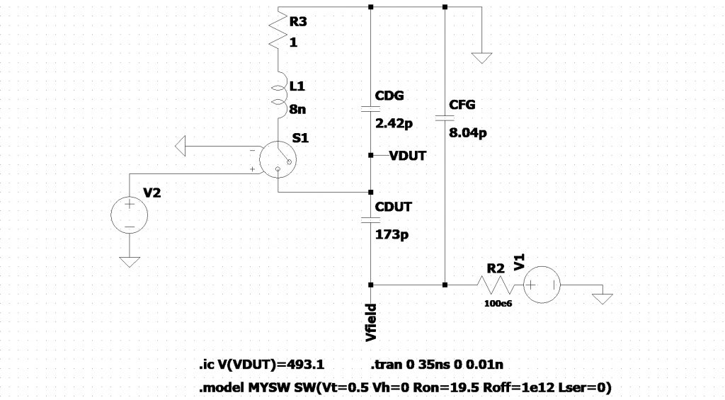
Figure 2 LTSpice circuit depicted for the 173 pF DUT
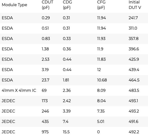
Table 1 Capacitance values from Atwood and calculated initial voltage for simulation. The ESDA modules consisted of a copper film on a thin piece of circuit board, similar to those used in the ESDA CDM standard. The JEDEC modules were round coins, similar t those used in the old JEDEC CDM standard. Both the ESDA and JEDEC standards have now been replaced by JS-002 which uses JEDEC type coin calibration modules. The integrated circuit was a 41 mm X 41 mm BGA with a metal heat sink on the top of the package.
Also, following Atwood, a value of 20.5 ohms was used for the combined 1-ohm sense resistor and spark resistance. The spark resistance was included as the on resistance of the relay. The value of inductance of 8 nH is somewhat larger than used by Atwood in his simulations, but the larger value better matches the waveform parameters in the FICDM standard JS-002 [4]. Table 1 also includes the calculated initial DUT voltage used in the simulations. The initial voltage was calculated from the series capacitance of CDUT an CDG with 500 V across the two capacitors.
Two simulated current waveforms are shown in Figure 3, for 3.19 pF and 173 pF modules, with a Field Plate voltage of 500 V. As would be expected, the CDM pulse for the smaller capacitance is smaller than the pulse for the larger capacitance. The small capacitor pulse width is also considerably narrower and less damped than for the large capacitor. What is surprising is that the despite the capacitance ratio of 68 between the two, the peak height varies by less than a factor of 2. The seemingly small difference between the waveforms can be understood if we consider how the CDM pulse is simply a redistribution of charge between the three capacitors when the DUT is grounded. The magnitude of the waveforms depends on relative values of the capacitors to each other, the difference between the state of voltages and charges on the capacitors before the CDM pulse, and the state of the voltages and charges on the capacitors just after the CDM pulse. While state of the voltages in the CDM system before the pulse are well understood, the voltage state just after the pulse are seldom considered.
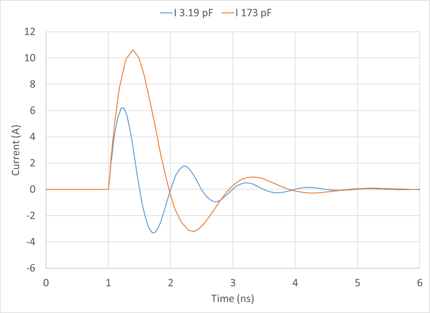
Figure 3 Simulated waveforms for CDUT 3.19 pF and 173 pF
Figure 4 shows the simulated DUT and Field Plate voltages, as well as the voltage across the CDUT capacitor, VCDUT, for the current pulses shown in Figure 3. The voltage on the DUT behaves similarly for the two DUT capacitances. The voltage starts off high, close to the charging voltage on the Field Plate, and drops to zero within 5 ns. The magnitude of the behavior for the Field Plate voltage and the voltage across CDUT are substantially different in magnitude, however.
For the 3.19 pF DUT the Field Plate voltage drops about 100 V while the voltage across CDUT increases from about 60 V to 400 V. In contrast, for the 173 pF DUT the Field Plate voltage drops by about 470 V while the voltage across CDUT increases from 7 V to just 29 V. The explanation is simple. For the 3.19 pF DUT the capacitor CFG is substantially larger than CDUT and can provide ample charge to CDUT when the DUT is grounded, while maintaining a high voltage on the Field Plate. For the 173 pF DUT the combined capacitances of CDG and CFG is 10.5 pF and just a small fraction of CDUT. The charge stored on CDG and CFG are therefore only able to change the voltage across CDUT a small amount, while the capacitor CFG is almost totally discharged.
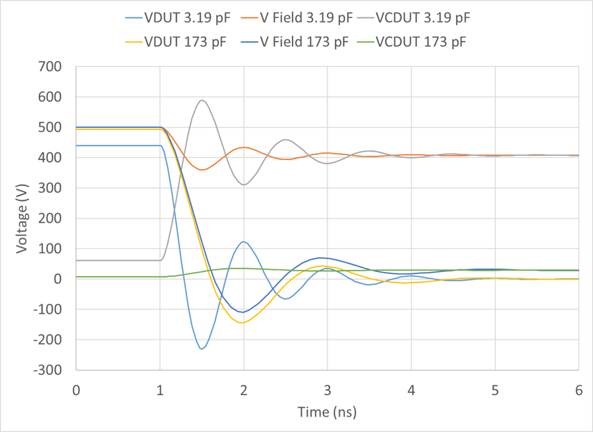
Figure 4 DUT and Field Plate voltage as a function of time for a DUTs with 3.19 pF and 173 pF values of CDUT
The amount of charge, and therefore the amount of current, in the CDM stress pulse depends on the relative sizes of the three capacitors. Figure 5 shows the simulated total charge in a CDM pulse as a function of CDUT. In the insert to Figure 5 a linear scale is used for the capacitance and it shows that for very low capacitance the charge increases approximately linearly with CDUT. As CDUT’s value approaches the value of CFG the amount of charge saturates. For larger values of CDUT a logarithmic scale is used for CDUT to show how the behavior for large CDUT
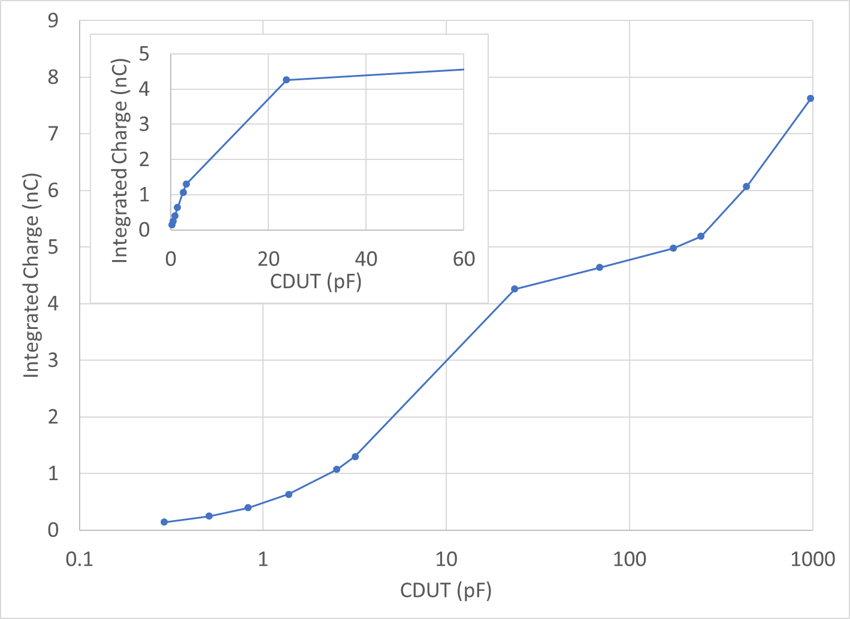
Figure 5 Simulated total charge in the CDM pulse as a function of CDUT
The joint JEDEC/ESDA standard for CDM, JS-002 [4] specifies four waveform parameters that must be met to qualify a FICDM tester, peak current, rise time, full width at half maximum and undershoot. We will not look at simulations of each of these parameters and see how they behave as a function of DUT capacitance. The parameters will also be compared to the waveform specifications from JS-002. In all cases the simulations fall within the experimentally determined waveform parameters in JS-002. This gives confidence that the simulations are a good representation of reality and are therefore useful for understanding the CDM event in FICDM testing
Figure 6 through Figure 9 show simulations of peak current, rise time, full width at half maximum and undershoot as a function of CDUT. In each of the figures the insert shows the behavior for low capacitance with a linear CDUT scale, while the main figure uses a log scale for CDUT for all capacitances simulated. All of the parameters show very sensitive dependence on CDUT for small CDUT, but saturation for large values of CDUT.
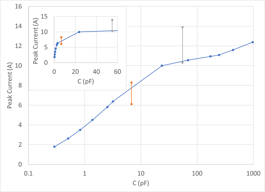
Figure 6 Simulated Peak Current as a function of CDUT. The vertical lines indicate the JS-002 specification limits.
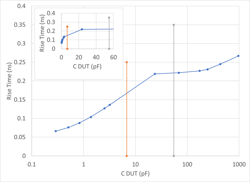
Figure 7 Simulated rise time as a function of CDUT. The vertical lines indicate the JS-002 specification limits.
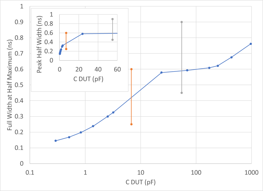
Figure 8 Simulated full width at half maximum as a function of CDUT. The vertical lines indicate the JS-002 specification limits.
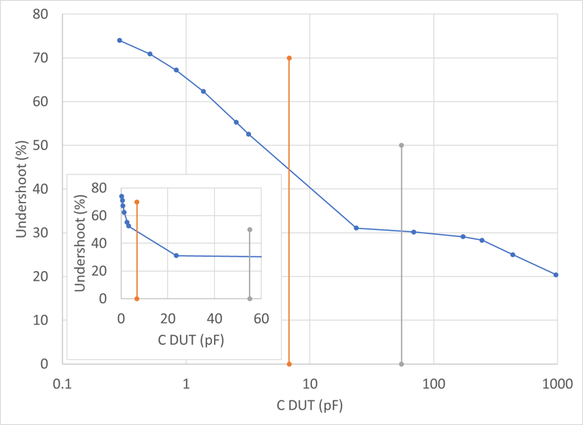
Figure 9 Simulated undershoot as a function of CDUT. The vertical lines indicate the JS-002 specification limits.
In this article the three-capacitor model for the field induced CDM ESD test method has been used to help understand the properties of the CDM test system. The model shows that during the CDM event currents that flow are the result of a redistribution of charge between the three capacitors in the CDM system. For small DUT to field plate capacitance, when CDUT is well below the capacitance CFG between the Field Plate and the Ground Plane, the currents are more sensitive to the value of CDUT. When CDUT approaches and becomes larger than CFG waveform properties become less sensitive to CDUT. The general trends as CDUT gets larger is that peak current increases, rise times get longer, width at half maximum increases and the amount of undershoot decreases.
[1] J. Montoya and T. Maloney, “Unifying factory ESD measurements and component ESD stress testing”, 2005 Electrical Overstress/Electrostatic Discharge Symposium,: 2005
[2] B. Atwood, Y. Zhou, Dave Clarke, and T. Weyl, “Effect of large device capacitance on FICDM peak current”, 29th Electrical Overstress/Electrostatic Discharge Symposium (EOS/ESD), 2007
[3] A. Wallash and L. Levit, “Electrical breakdown and ESD phenomena for devices with nanometer-to-micron gaps”, Proc. SPIE V4980, 2003, pp. 87-96.
[4] ANSI/ESDA/JEDEC JS-002-2018, “For Electrostatic Discharge Sensitivity Testing Charged Device Model (CDM) – Device Level” 2018
FEBRUARY 12, 2020 BY ROBERT ASHTON and STEPHEN FAIRBANKS
This will be a different type of blog. I will primarily be pointing to two recent articles I have written which appeared in In Compliance magazine. The following paragraph is how In Compliance magazine describes itself in the About section of their web site.
"In Compliance is committed to delivering information that impacts electrical/electronics engineers in their daily work. We provide coverage of regulatory compliance issues, technical explanations and guidance, and inspiring new developments and technologies."
I recommend this magazine, it has a lot if interesting articles, and best of all it is free, with the usual registration for trade magazines. Check it out at https://incompliancemag.com/.
The Electrostatic Discharge Association (ESDA) has a regular column in the magazine on ESD and related standards and issues called “Hot Topics in ESD”. The articles are usually in a Question and Answer format. The article in the August 2019 issue was on Cable Discharge Event (CDE) and the November article was on pin combinations in Human Body Model (HBM). In the next two sections I will discuss what is presented in the two articles, as well as provide links to the full articles.
CDE occurs when a cable (ethernet, USB, HDMI, etc.) becomes charged and discharges into a system when plugged in. CDE is often described as being similar to a transmission line pulse system, but this is an oversimplification. The articles explains some of the issues involved in cable discharge and can be found at: https://incompliancemag.com/article/esda-working-group-14-system-level-esd/
HBM testing is performed by stressing a single pin on an electronic device versus one or more other pins on the device. In the joint JEDEC/ESDA HBM standard JS-001 there is a choice between two tables describing the required pin combinations. Table 2B is the traditional set of pin combinations from the earlier JEDEC and ESDA HBM standards. Table 2A is a new set of pin combinations, which can significantly reduce the number of individual stresses to the device under test, saving test time and reducing wear out. The price for using Table 2A is the need for increased knowledge of the device being tested. The HBM article in In Compliance gives practical guidance for choosing which pin combination table to use. It is also the only technical article that I know which has a reference to William Shakespeare. The article can be found at: https://incompliancemag.com/article/hbm-pin-combinations/
OCTOBER 23, 2019 BY ROBERT ASHTON and STEPHEN FAIRBANKS
This blog post is an update of an article originally published in 2008 in the now defunct Conformity magazine. The original article is available elsewhere on the Minotaur Labs web site, but changes in the test standards for electrostatic discharge (ESD) have changed sufficiently to warrant a “freshening” of the article. Since that time Machine Model (MM) has largely been dropped as a test method and the JEDEC and Electrostatic Discharge Association (ESDA) CDM test standards have been merged into one standard and the Automotive Electronics Council (AEC) CDM standard now references the joint JEDEC/ESDA CDM standard rather than the old ESDA standard.
Integrated circuits are commonly tested for ESD robustness with 2 tests, Human Body Model (HBM) and Charged Device Model (CDM). Most engineers quickly grasp the procedure for HBM, but the CDM test is often poorly understood. This is unfortunate, because a large fraction of the ESD failures experienced in modern board assembly operations are CDM type failures. This article will describe the events which occur during a CDM test conducted using the widely accepted field induced CDM (FCDM)[1] test.
All ESD events consist of a charged object discharging through a discharge path. Characterizing an ESD event requires understanding both the capacitance and the discharge path. HBM can be described with the simple circuit diagram in Figure 1. This procedure works well because this test standard emulates a person becoming charged and discharging through the sample being tested. The capacitance of a person is approximately 100 pF and the discharge path for a human includes skin and body resistance, which is approximated by a 1500 Ω resistor. CDM is different. CDM emulates an integrated circuit that becomes charged during handling and discharges to a grounded metallic surface. The capacitance is the capacitance of the integrated circuit to its surroundings and the discharge path is a pin of the IC directly to a grounded surface. The test method for CDM must have a capacitance that scales with the device under test’s (DUT) capacitance and a discharge path with very little impedance other than the DUT’s own pin impedance and the resistance of the resulting arc. In CDM the stress is dominated by the properties of the device being tested, while in HBM the stress is dominated by the source of the stress, a charged person. The field induced CDM test setup is designed to allow the properties of the DUT to dominate the stress.
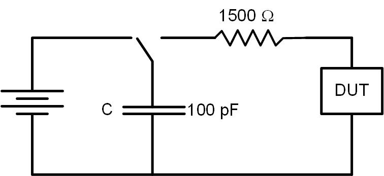
Figure 1 Basic circuit diagram used to describe HBM and MM
Figure 2 shows a representation of an FCDM simulator. The simulator consists of a metallic field plate covered with a thin layer of FR4 or similar circuit board material. The potential of the field plate can be controlled with a high voltage power supply through a high value resistor. Suspended above the field plate is a ground plane. At the center of the ground plane is a spring loaded pogo pin. The pogo pin is connected to the ground plane with a low inductance 1 Ω resistance to provide a current sense element. The pogo pin and ground plane are also connected to a 50 Ω coaxial cable. The separation between the field plate and the ground plane as well as the relative position of the ground plane over the field plate is computer controlled.
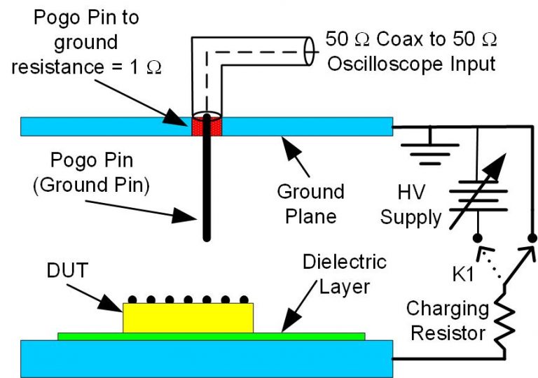
Figure 2 Field Induced Charged Device Model Simulator
Placing the DUT with the pin side up (dead bug position) produces a capacitance between the DUT and the field plate that scales with the size of the DUT. A low inductance discharge path to ground is formed by moving the ground plane relative to the field plate such that the pogo pin can touch any pin on the DUT. The 1 Ω resistor and coaxial cable provide a low inductance current sensor so that discharge waveforms can be conveniently measured. The process of “charging” and “discharging” the DUT is where most of the confusion over FCDM occurs. Confusion about the test procedure is understandable because the actual process is opposite from what is expected. It is often stated that in FCDM the DUT is inductively charged and then discharged by contacting the pogo pin to the DUT. In fact, field induction does not place any charge on the device. Also, the “discharge” when the pogo pin first touches the DUT is when the DUT is actually charged.
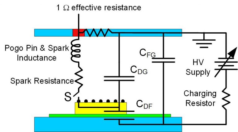
Figure 3 Capacitors added to field induced CDM simulator
In Figure 3 a circuit diagram is overlaid on top of a simplified version of the FCDM simulator. This circuit is a simplification of the full circuit but shows the most important features. A very thorough theoretical treatment of FCDM testing is provided by Atwood et. al.[2] CDF is the capacitance of the DUT to the field plate, CDG is the capacitance of the DUT to the ground plane and CFG is the capacitance of the field plate to the ground plane. Touching the pogo pin to a pin on the DUT has been represented by the switch S. Key to the understanding of FCDM is the series capacitors CDUT and CDG. Assuming no initial charge on the DUT, with the switch S open the DC voltage between the DUT and the Field Plate is:
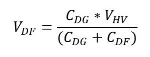
Because the separation of the DUT from the field plate is always much less than the separation of the DUT from the ground plane; CDF is always much larger than CDG. The voltage between the DUT and the field plate, VDF, will be small and the DUT potential will therefore closely track the power supply voltage. The potential of the DUT relative to the ground plane can therefore be controlled without actually putting any net charge on the DUT.
Because the separation of the DUT from the field plate is always much less than the separation of the DUT from the ground plane; CDF is always much larger than CDG. The voltage between the DUT and the field plate, VDF, will be small and the DUT potential will therefore closely track the power supply voltage. The potential of the DUT relative to the ground plane can therefore be controlled without actually putting any net charge on the DUT.
A sample FCDM waveform for a small JEDEC calibration module is shown in Figure 4. The waveform shows the typical CDM characteristic; a very high current short duration pulse.
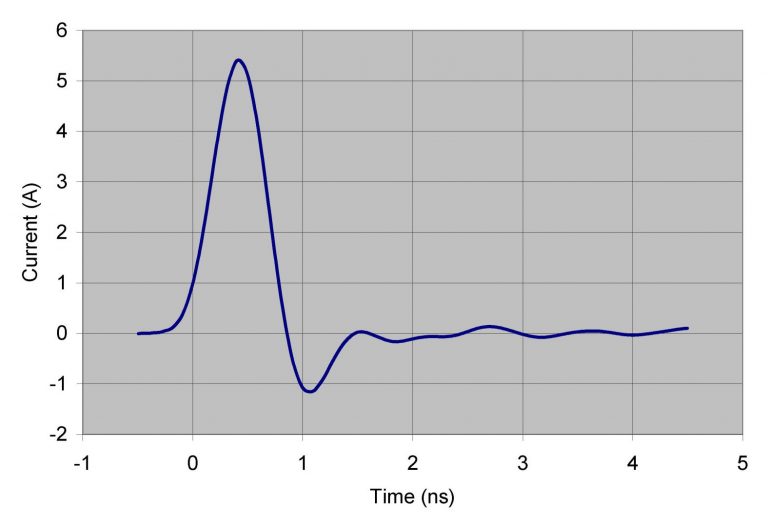
Figure 4 Field Induced CDM waveform of a small JEDEC Module at 500 V
The dual pulse procedure continues after step 5 of the single polarity procedure.
6. Without changing the voltage on the HV power supply the distance between the field plate and the ground plane is increased so that the pogo pin separates from the DUT pin. The DUT is still charged and will stay at approximately zero volts while the field plate is at the HV power supply voltage.
7. The potential on the field plate voltage is slowly returned to zero by setting the HV supply to 0 V. Changing the field plate potential to zero volts does not change the fact that there is a nearly 500 V potential across the capacitor CDF. The result is that when the field plate reaches zero volts, the DUT potential is close to -500 V.
8. At this point the separation of the field plate and ground plane is decreased until an arc forms between the pogo pin and the DUT pin, rapidly grounding the DUT. This results in a second stress pulse with approximately equal amplitude as the first, but opposite polarity.
9. After a suitable delay, to allow the field plate to return to zero volts after the arc, the separation between the field plate and the ground plane is increased and the test sequence is complete. Further stresses can be performed on the same pin or testing can be continued on other DUT pins.
The dual pulse method can save some time during FCDM testing.
The joint JEDEC/ESDA standard JS-002-2018 is the most widely used CDM test method. The Automotive Electronics Council (AEC) Q100-011 test method is based on the JS-002 standard, but has several additional requirements for automotive applications. The IEC CDM standard, IEC 60749-28 Ed.1, is mostly a copy of the JS-002 CDM standard. (IEC 60749-28 Ed.1 also includes an Annex which describes a direct, rather than field induced, charging method which follows the Japanese, JEITA EIAJ ED-4701/300 Test Method 305. This test method does not necessarily produce the same results as the field induced CDM method of JS-002.)
FCDM is an extremely valuable test method for ensuring that integrated circuits can survive in a modern, automated manufacturing environment. The test method creates a capacitance that scales with DUT size and a low impedance discharge path, providing a good simulation of real CDM events.
[1] ANSI/ESDA/JEDEC JS-002-2018 “For Electrostatic Discharge Sensitivity Testing Charged Device Model (CDM) – Device Level.
[2] B.C. Atwood, Y. Zhou, D. Clarke, T Weyl, “Effect of Large Device Capacitance on FICDM Peak Current” EOS/ESD Symposium, 2007.
AUGUST 7, 2019 BY ROBERT ASHTON and STEPHEN FAIRBANKS
The qualification requirements for integrated circuits for both JEDEC [1] and the Automotive Electronics Council (AEC) [2], require ESD testing for both Human Body Model (HBM) and Charged Device Model (CDM). Despite this requirement, examination of integrated circuit datasheets often does not include ESD data, and when they do it is overwhelmingly HBM data, with CDM data seldom included. The Electrostatic Discharge Association’s device testing working group 5.0 found the lack of ESD data, and especially the lack of CDM data troubling enough that it recently published a Standard Practice Document [3] recommending a format for reporting ESD data in datasheets. In the recommended format the CDM data format was placed before the HBM data format, and that was not just due to alphabetical order. It was to emphasize the importance of CDM data. The lower representation of CDM with respect to HBM is also reflected in Minotaur Labs experience. We receive about twice as many requests for HBM testing as for CDM testing.
So, why perform CDM testing if the industry appears to treat it as less important than HBM? This blog post will try to explain why CDM represents a real threat to integrated circuits in a modern manufacturing environment. We will start with a very traditional explanation of a CDM event, but then will discuss how this relates to a today’s manufacturing environment.
The classic example of a CDM event is shown in Figure 1, a shipping tube of integrated circuits is dumped onto a grounded metal bench. Depending on the material of the integrated circuit (IC) and the anti-static properties of the shipping tube the IC can become charged with value Q. The voltage of the integrated circuit depends on the charge on the IC and its capacitance with respect to the metal table, CDUT. Since the capacitance between the IC and the table’s surface is likely small, pF range, the IC to table voltage can become quite large, hundreds of volts.
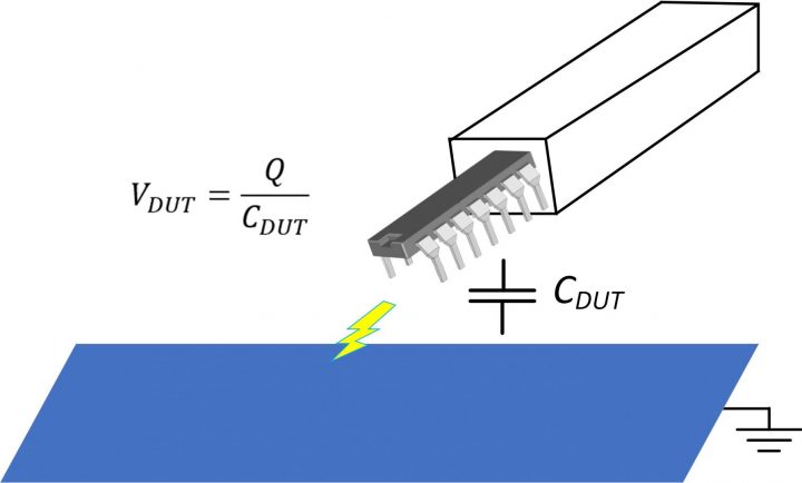
Figure 1 Traditional idea of a CDM event, integrated circuits in a shipping tube are dumped onto a grounded metal surface
As the IC drops toward the table CDUT will get larger while VDUT gets smaller. If VDUT started at hundreds of volts there will likely be an air breakdown between the IC and the table top before contact is made. The nature of the discharge can be estimated with a simple LCR circuit. We expect the capacitance to be small, so we will assume 1 pF. There will also be inductance. The inductance will be for both the leads on the IC as well as inductance of the arc. Using the rule of thumb for inductance of a trace being 1 nH per mm we will assume a 1 nH inductance. We expect the metal resistance of the table and the IC to be quite small, so that arc resistance will dominate. Arc resistance for a small spark is often on the order of about 20 ohms. From this we can do a SPICE simulation to give an estimate of a CDM event, which is shown in Figure 2. What we see is an extremely fast event, lasting less than half a nano second, but having a current approaching two amperes.
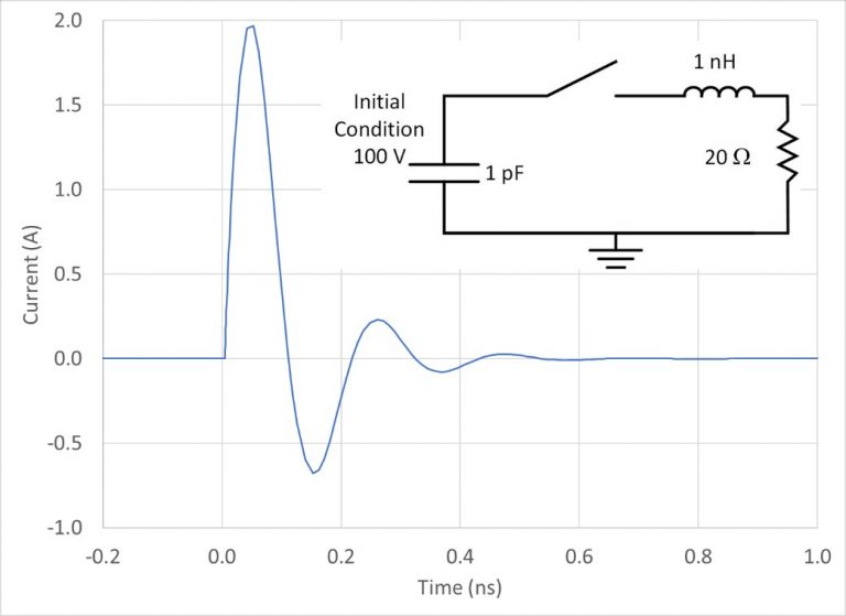
Figure 2 SPICE simulation of a charged integrated circuit discharging to a metal table.
This result is very similar to the current and time durations of currents in the CDM test and can definitely damage integrated circuits. It is fair to ask, however, who in a modern manufacturing environment dumps a shipping tube of ICs onto a metal table. The answer is of course, no one, but the current pulse above is very similar to what can be expected with modern manufacturing methods.
The heart of most circuit board assembly operations is the “Pick and Place” machine. These robotic machines use vacuum pickup heads to grab surface mount devices, including integrated circuits, resistors, capacitors and other components and place them on a circuit board which has already had solder past applied to bond pads. For economic reasons Pick and Place machines must work at high speed. If you are not familiar with these machines it is instructive to watch a video of the machines in action. One that I particularly like is at https://www.youtube.com/watch?v=S8qkaTsr2_o. A more comprehensive overview of the board assembly process is available at https://www.youtube.com/watch?v=BepAMlrJwXI.
The bottom line for CDM is that with machines with a large number of moving parts it is very easy for charge to build up either on the circuit board or on an IC being moved from tape and reel, shipping tubes or shipping trays, to the circuit board. Manufacturers of Pick and Place machines go to great lengths to prevent charge buildup in their machines, but with so many mechanical parts moving so quickly, some charge buildup is inevitable.
The question is then, do we expect the ESD events in a Pick and Place machine to be similar to what we discussed earlier? Figure 3 shows a cartoon of a Pick and Place machine in action. The situation is very similar to the scenario in Figure 1. If the IC has become charged a CDM pulse similar to that shown in Figure 2 could occur. The biggest difference is that since the IC is being placed flat on the circuit board surface the capacitance is likely larger than a corner of an IC touching down first.
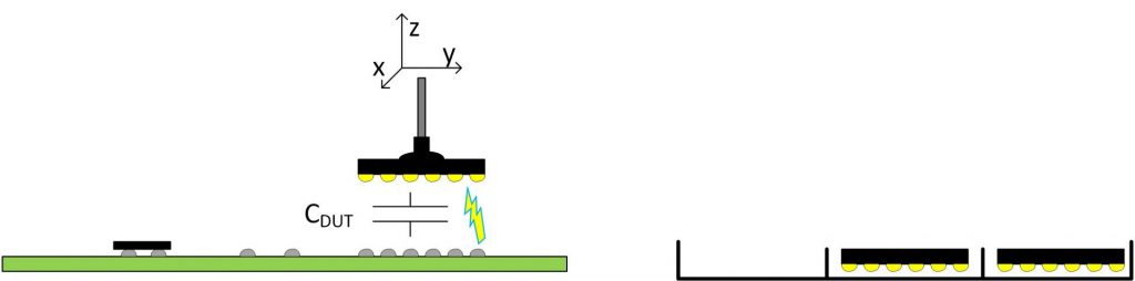
Figure 3 Cartoon of a pick and place machine listing an IC from a shipping try and about to place it on a circuit board with solder past applied and some other components already placed
An important thing to remember is that the IC need not be charged for a CDM event to occur. A circuit board that is charged will stress the IC in the same way as if the IC is charged. The only difference is that if the board is charged positive with respect to the IC it creates the same stress as if the board were grounded and the IC was charged negative. The severity of a CDM event depends on the following factors; the relative potentials between the two objects when the discharge occurs, the capacitance between the IC and the circuit board and the impedance, resistive and inductive, between the circuit board and the IC.
In summary, any time an integrated circuit makes metal to metal contact with an object at a different potential a CDM event will occur. This type of event is much more prevalent in a modern manufacturing environment than a person touching the IC. Verifying the CDM robustness of an IC is therefore very important for ensuring that it will be a robust component during manufacture.
[1] JESD47I.01 “Stress-Test-Driven Qualification of Integrated Circuits”
[2] AEC – Q100 – REV-H “Failure Mechanism Based Stress Test Qualification for Integrated Circuits”
[3] ANSI/ESD SP5.0-2018 “Reporting ESD Withstand Levels on Datasheets”
APRIL 19, 2019 BY ROBERT ASHTON and STEPHEN FAIRBANKS
In previous blog posts I discussed the Human Body Model (HBM) waveform and traditional HBM pin combinations. In this post I will discuss the updated pin combinations available in the HBM standard JS-001 2017 and the motivations for those pin combinations. Unless you are familiar with the traditional HBM pin combinations I would suggest that you read the traditional pin combination blog before continuing the current blog.
The traditional pin combinations, as presented in Table 2B of JS-001 2017, were developed in the 1980s. Even at that time it was recognized that stressing each pin versus every other pin one at a time would create very long test times. To create a more reasonable set of pin combination the traditional pin combinations were developed. The traditional pin combinations are in Table 2B of JS-001 and are reproduced in Table 1 below. In Table 2B each power supply domain was attached to terminal B (ground side) and all other pins were stressed to that pin one at a time. After cycling though all of the power supply domains being connected to the B terminal, each non-supply pin was stressed versus all other supply pins tied together. The traditional pin combinations kept test times to reasonable levels, and they served the industry very well for many years. Over the last 20 years, however, pin counts have continued to increase and, in some ways even more significant, the number of power supply domains have increased dramatically on some high pin count devices.
There are three basic issues with the traditional pin combinations in today’s high pin count devices:
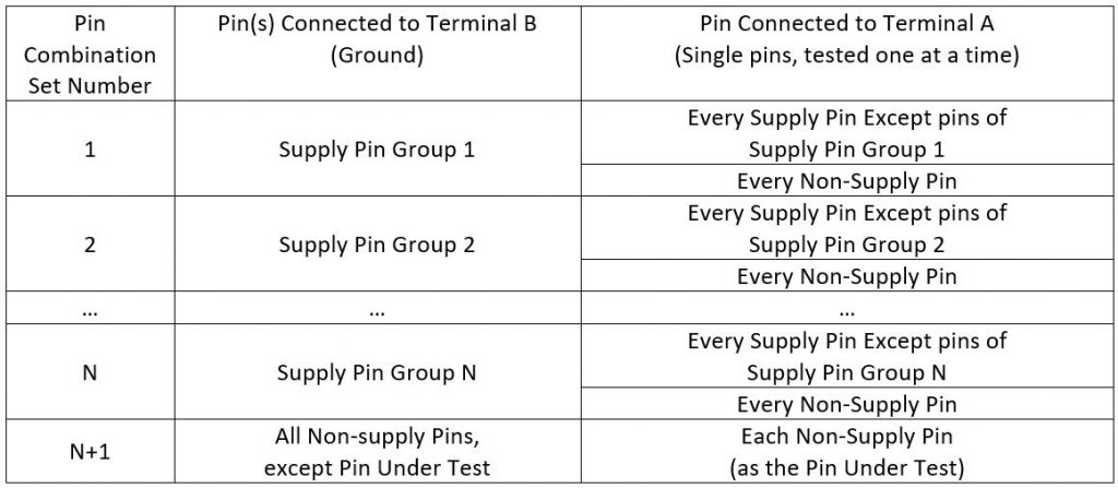
Table 1 Reproduction of JS-001 Table 2B. (Notes not relevant to the present discussion are not included for clarity, but are important for compliant HBM testing.)
Consider Figure 1, which presents a simplified representation of an integrated circuit with multiple power domains. Not shown is that the VDD1/VSS1 section of the circuit will have multiple inputs, outputs and bidirectional buffers. Also not shown is that each of the other VDDx/VSSx sections of the circuit are likely to have multiple inputs and outputs as well. Note that VSS and GND busses are considered power domains for HBM testing.
When input I1 is stressed positive versus VSS1 in Figure 1 the current flows through the steering diode to VDD1, down through the VDD1 to VSS1 protection circuit and finally out through the VSS1 line. Stressing input I1 to any of the other VSSx pin groups exercises this same path again, in addition to flowing through the isolation diodes and finely to the VSSx lines. This shows that as power domains, either VDDx or VSSx, are added the required number of HBM stresses increases. For example, if an integrated circuit has 300 IOs and a small power section is added with a single VDDx pin and single VSSx pin, 1200 additional HBM stresses are added to the pin combinations, 300 positive and 300 negative stress to both VDD and VSS.
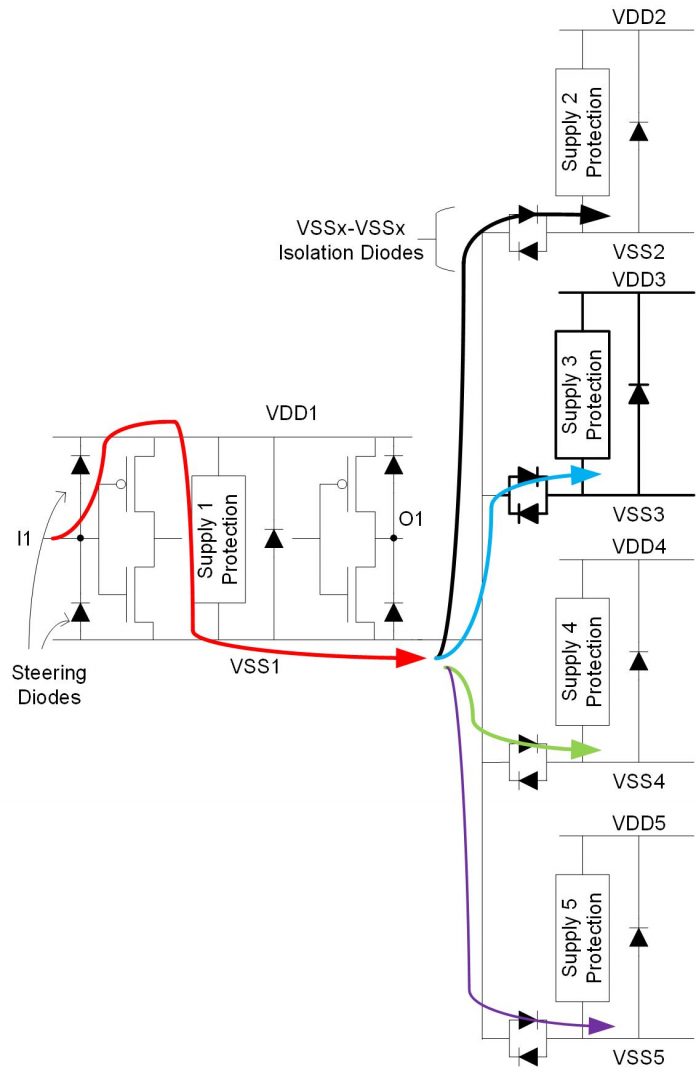
Figure 1 Illustration of the multiple stresses which an input pin is subjected to when stressed positive with respect to various VSS pin groups
As the total number of stresses increases due to additional power domains certain circuit elements get stressed multiple times. For example, in Figure 1 Supply 1 Protection is stressed every time there is a positive stress to any IO powered by VDD1 and VSS1 with respect to VSS1 or to any VSSx or VDDx other than supply region 1. Similarly, the isolation diodes between different VSSx regions will be stressed multiple times for any cross-power supply stresses. These repeated stresses can lead to wear out of these elements as hundreds or even thousands of stresses are applied to the same circuit element.
It is tempting to say that all circuit elements in an ESD path should be able to survive repeated stresses, but this is neither practical or necessary. HBM testing is intended to ensure that an integrated circuit can survive manufacture in an ESD controlled manufacturing facility. Under these conditions an integrated circuit is expected to only experience at most several ESD stresses during its manufacturing process. Testing to survive hundreds or thousands of repeated stresses is not realistic or necessary.
The final test called out for in Table 2B of JS-001 2017, see Table 1 requires that each non-supply pin be stressed versus all other non-supply pins tied together. The experience of the members of the HBM working group was that this test very seldom produces failures, and why continue to do a test which never fails? As will be explained in Section 3.2, it is not surprising that this pin combination seldom fails in a way not detected by other pin combinations.
In summary, for high pin count integrated circuits with a large number of separate power supply groups the pin combinations resulted in excessive test time and can create wear out of some parts of the ESD protection network due to being stressed hundreds or even thousands of times. Additionally, the non-supply pin to all other non-supply pin tests seldom create failures and is usually not a value-added test.
There are two fundamental changes in JS-001 Table 2A from the traditional pin combinations in Table 2B and these are shown in Table 2 which shows the edits required to change Table 2B into Table 2A. The first change is that non supply pins are only stressed to power supply groups that are “associated” with the non-supply pin being tested. The second is that each non-supply pin is no longer stressed with respect to all other non-supply pins tied together. The only non-supply to non-supply stressing required is if two non-supply pins are “coupled” with each other. We will discuss these two changes separately.
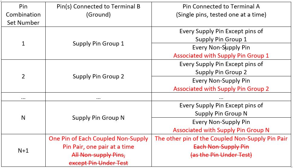
Table 2 Reproduction of JS-001 Table 2A showing the differences from the traditional pin combinations in Table 2B. In rows 1 through N the only differences between JS-001 Tables 2A and 2B is the text in Red added to Table 2A. In row N+1 the original Table 2B wording is in Red and crossed out. (Notes not relevant to the present discussion are not included for clarity, but are important for compliant HBM testing.)
The key to understanding why it makes sense to only stress non-supply pins to “associated” power pin groups is understanding how some complex pin combinations are a combination of other less complex pin combinations. For example, see Figure 2 which illustrates how a positive stress from I1 to VDD2 is made up of several simpler pin combinations. The individual stresses are described in Table 3. In fact, there are multiple ways in which the full positive I1 to VDD2 current path is exercised with other pin combinations in Table 2B of JS-001. The full list of possibilities is listed in Table 4.
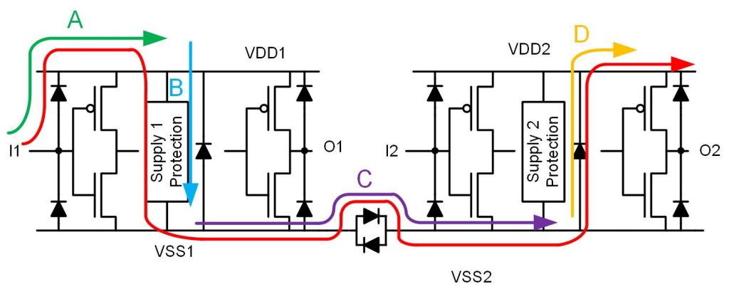
Figure 2 Illustration of how a stress from I1 to VDD2 is a combination of other stresses combinations also tested
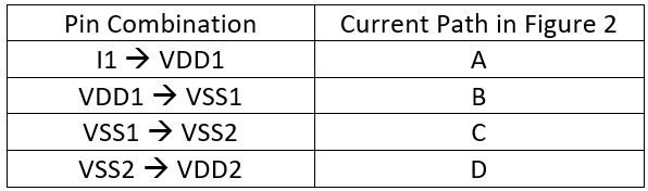
Table 3 Description of elemental pin combinations which make up a positive I1 to VDD 2 stress
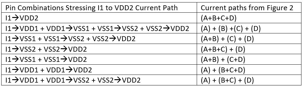
Table 4 Pin Combinations which exercise positive stress path from I1 to VDD2. In column 1, XX→YY represents a traditional pin combination from JS-002 Table 2B. Column 2 shows how these same paths using the current path designations from Figure 2. Current paths in parentheses are those done in a single stress.
Table 4 shows that there is considerable redundancy in testing the current path for positive stress of I1 with respect to VDD2. The new pin combinations in JS-001 Table 2A take advantage of this redundancy to reduce stress time and overstress. Table 2 shows that in lines 1 through N the only difference between JS-001 Table 2A from Table 2B is the addition of the phrase “Associated with Supply Pin Group X”.
Non-Supply Pins “associated” with a particular Supply Pin Group are non-supply pins which are powered by the Supply Pin Group in question. For example, in Figure 2, I1 and O1 are “associated” with supply pin groups VDD1 and VSS2, while I2 and O2 are “associated” with supply pin groups VDD2 and VSS2. Eliminating stressing to non-associated power pin groups would mean that I1 would no longer be directly stressed with respect to VDD2 or VSS2. Table 5 reproduces Table 4, but shows which stresses in the I1 to VDD2 current path are no longer specifically stressed with JS-001 Table 2A. The change looks very minimal but gives a large improvement in overall test time and reduction of repeated stressing of a number of elements in the protection design.
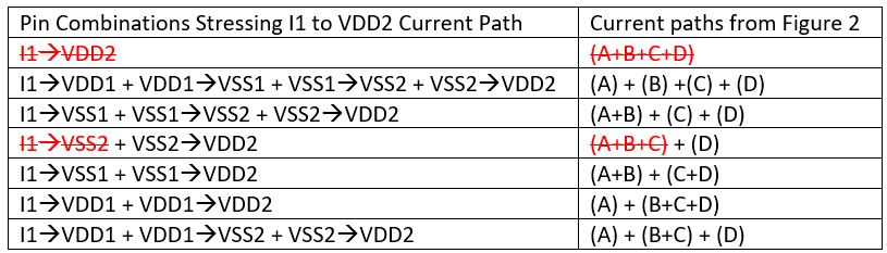
Table 5 Reproduction of Table 4 showing stress combinations in the I1 to VDD2 current path no longer done with JS-001 Table 2A that are in Table 2B.
It is of course important to ask if the elimination of the stressing to non-associated supply pin groups opens up a high probability of missing weakness in the ESD design. Experience of the HBM working group is that HBM failures for stresses such as I1 to VDD2 were invariably also found in a stress from I1 to VSS1 or in stress of VDD1 to VDD2. This makes physical sense.
ESD design weaknesses fall into two categories, weakness in the intended ESD current path, or layout issues creating a current path outside of the intended ESD current path. Let’s consider the I1 to VDD2 example from Figure 2. If there is a weakness in the intended current path that weakness should be seen in one or more of the pin combinations which make up the I1 to VDD2 current path. Table 5 shows that the elements of the I1 to VDD2 path are still stressed multiple times even with the elimination of stress to non-associated power pin groups.
The other possible failure mode is that there is a specific weakness in the design or layout at input I1. If that is the case it is very unlikely that the only pin combination that will see it is I1 to VDD2, since VDD2 is likely in an entirely different region of the integrated circuit. In fact, the most likely stresses to find a weakness in the I1 design are stresses to its associated power groups, VDD1 and VSS1. This matched the experience of the HBM working group when it developed JS-001 Table 2A.
The traditional pin combinations, JS-001 Table 2B, required each non-supply pin to be stressed to all other non-supply pins tied together. This was sometimes called the “pin to the world” test. Experience of the working group was that this pin combination essentially never produced failures, or at least never produced failures not seen when stressing non-supply pins versus supply pin groups. This is not a surprising outcome if the expected current paths are examined, as shown in Figure 3
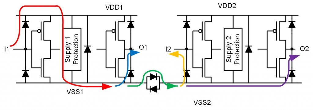
Figure 3 Current paths expected when stressing pin I1 versus all other non-supply pins
Figure 3 shows the current paths for a positive stress of I1 versus all other non-supply pins. The current begins with a well-defined path, through the steering diode to VDD1 and then through Supply 1 Protection to VSS1. The current then begins to spread out. The current can flow to all other non-supply pins connected to the power domain VDD1-VSS1 such as O1 as well as all non-supply pins on all other power domains. The only path which sees the full stress current is between I1 and VSS1, which is already stressed separately.
There was therefore considerable sentiment to eliminate all non-supply pin to non-supply pin testing. This was not done because it is known that some “coupled” non-supply pins could be weak when stressed versus each other. The JS-001 definition for a coupled non-supply pin pair is as follows:
Two pins, such as differential amplifier inputs, or low-voltage differential signaling (LVDS) pins, that have between them an intended direct current path, such as a pass gate or resistor.
Based on this the HBM working group replaced the more general non-supply to non-supply stress with stress only between coupled pairs of non-supply pins. This reduces the amount of non-supply to non-supply stressing considerably and focuses on pin combination that could be weak.
The use of the new pin combinations in JS-001 Table 2A considerably reduces test time and excessive stress for high pin count integrated circuits which have a high number of power supply groups. It is important to note that both Table 2A and Table 2B are acceptable for use in HBM testing. Which pin combination to use for HBM testing of a specific integrated circuit is a mix of engineering judgement and a business decision. I will discuss this in an upcoming blog post.
NOVEMBER 21, 2018 BY ROBERT ASHTON and STEPHEN FAIRBANKS
Traditionally there have been three test methods for evaluating the robustness of integrated circuits to electrostatic discharge (ESD) damage during manufacturing, Human Body Model (HBM), Machine Model (MM) and Charged Device Model (CDM). Recently MM has fallen out of favor and is no longer a requirement nor accepted test for qualification based on either the JEDEC’s JESD47I or the Automotive Electronics Council (AEC) Q100. Many OEMs, however, have a long history of requiring MM testing and are reluctant to give up on a test that they believe has served them well. It is reasonable, in an era in which almost all manufacturing is done using automated equipment, that a test with the name Machine Model should be an important ESD test.
In this blog it will be shown that Machine Model does not represent the type of stress which occurs in a manufacturing line and the information that it provides is redundant to HBM.
MM was originally developed in Japan, but the name Machine Model was not used by the original developers. [1] The original intention was to create a human body ESD test which did not require the high voltages required during HBM testing. The name Machine Model was given to it by others, probably in the United States. The assumption was, since there was no explicit resistor in the model the results would be similar to what would occur in a low resistance, metal to metal contact. The problem, is that the stress waveform produced by the MM test method does not represent the most important aspects of a metal to metal contact.
The MM equivalent circuit is usually represented as shown in Figure 1, a 200 pF capacitor discharging directly into the device under test (DUT) [2]. The ESDA MM test method [3] includes a 0.75 uH inductor and a 10 Ohm resistor in the schematic for reasons that will be clear when we look at the required waveforms. During waveform qualification and verification of the MM tester the DUT is replace by a short and a 500 Ohm load. Representative waveforms for those two cases are shown in Figure 2 and Figure 3 and the required waveform parameters in the JEDEC standard are shown in Table 1.
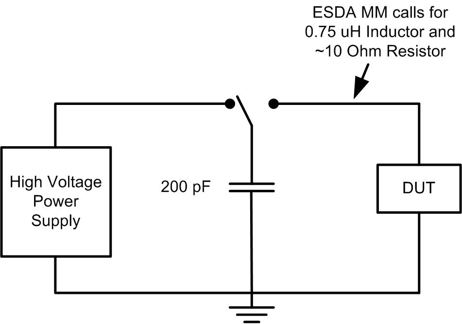
Figure 1 Circuit diagram often used to represent Machine Model. In the ESDA version the pulse source is represented only as a box with the text, 200 pF and 0.75 uH.
Figure 2 Required current waveform for a short from JEDEC MM standard (from JESD 22A115C)
Figure 3 Required current waveform through 500 ohm resistor from the JEDEC standard (from JESD 22A115C)
Table 1 Waveform parameters from the JEDEC MM standard (from JESD 22A115C)
Even after a casual observation the waveforms do not look particularly like what would be expected from the circuit diagram in Figure 1 and the inductor and resistor included in the ESDA test method begin to make sense. The damped oscillation implies the required inductor and resistance. Using the equation for the resonant frequency of an inductor – capacitor circuit,
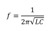
with 200 pF and 0.75 uH predicts a frequency of 13 MHz, near the middle of the frequency range in the JEDEC MM standard.
The large oscillations in the 500 Ohm waveform is not however predicted by either the JEDEC or ESDA schematics. A 200 pF capacitor discharging through a 0.75 uH inductor and 510 Ohms of resistance predicts a sub 10 ns rise time followed by an exponential decay with a 100 ns time constant. The large oscillations seen in Figure 3 would not be expected. It is therefore obvious that the traditional schematic shown in Figure 1 leaves out important circuit elements. A simple LTSpice simulation can give us a much better understanding of the true schematic of a MM simulator.
(Note, there is no requirement that the oscillations in the 500 Ohm waveform in Figure 3 be present. As will be shown below, they are caused by unavoidable parasitics in a realistic MM tester.)
Simulations of MM were performed using the schematic in Figure 4. This schematic includes the 0.75 uH inductance and 10 Ohms included in the ESDA test method. What is added is a lumped, 20 pF, parasitic capacitance between the inductor and ground. The results for 400 V are shown in Figure 5 for a short (0.1 Ohm) and Figure 6 for 500 Ohms. The results are similar to those in Figure 3 and Figure 4. The biggest difference is that the simulation shows a high frequency ring in the Short simulation. This high frequency ring is actually present in the sample Short waveform in the ESDA test method. The placement of Capacitor C2 determines if there is a high frequency ring in the short waveform. If C2 is placed directly across RDUT there is no high frequency ringing in the Short simulation, but the oscillation remains in the 500 Ohm simulation.
Figure 4 Schematic of LTSpice simulation of MM
Figure 5 Simulation of 400 V MM through a 0.1 Ohm resistor
Figure 6 Simulation of 400 V MM through a 500 Ohm resistor
The best measurements of what a “real word” machine, metal to metal, contact were reported in 2003 at the EOS/ESD Symposium by Jon Barth and his co-authors. [4] They charged large metal frames to voltages up to 200 V and discharging them into a high bandwidth current measurement target. Sample results are shown in Figure 7. The results show a fast rise time initial pulse, followed by ringing with a frequency of about 63 MHz. The measured ringing, although at a higher frequency than the approximately 13 MHz of MM, shows at least some similarity to MM. The initial spike, which is a far more severe stress than the ringing which follows, is not represented in MM at all. The expanded time scale on the bottom of Figure 7 shows the rise time of the initial pulse to be on the order of 100 ps.
The rapid rise and magnitude of the initial current spike in the Barth measurements casts into question the validity of the MM test method as a predictor of ESD performance during real metal to metal ESD events. Simulations predict a 10 to 90 % rise time for MM testing of almost 12 ns. This is even longer than the 2 to 10 ns rise time allowed during HBM testing.
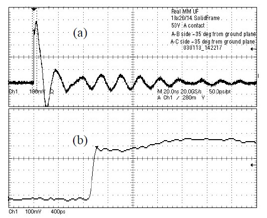
Figure 7 Figure 6 from Barth paper. Top figure is 20 ns per division and the bottom figure shows the initial current rise at 400 ps per division
The main feature of the real metal to metal contact, the initial current spike much more closely matches a Charged Device Model (CDM) test than the MM test. The question then remains, does MM provide additional information not covered in the Human Body Model test?
The Industry Council on ESD Target Levels studied this issue extensively. As reported in [1], HBM testing always provides a level of MM robustness. In all of the analysis that the Industry Council they found no field return data which indicated that a field return could be reproduced with MM that could not also be replicated by HBM. This is not true for CDM. Charged device model usually creates distinct failure mechanism from HBM and MM failure signatures. CDM failure signatures also more closely resemble the types of failures seen in a manufacturing environment than HBM and MM failure signatures.
It has been shown that the MM test method does not represent the real threat from a metal to metal contact due to the large inductance required to meet the waveform requirements. The fast rise time of a metal to metal contact is reproduced more accurately with the CDM test method. Additionally, MM is redundant with respect to HBM in terms of rise time, pulse duration and the failure modes detected. The performance of MM testing on integrated circuits is not a value-added test method and should not be used.
[1] Charvaka Duvvury, “Discontinuing Use of the Machine Model for Device ESD Qualification”, In Compliance Magazine, July 1, 2012. Available at: https://incompliancemag.com/article/discontinuing-use-of-the-machine-model-for-device-esd-qualification/
[2] JEDEC JESD22-A115C, “Electrostatic Discharge (ESD) Sensitivity Testing, Machine Model (MM)”, November, 2010. (This document is no longer available on the JEDEC web site.)
[3] ANSI/ESD STM5.2-2012, “Standard Test Method for Electrostatic Discharge (ESD) Sensitivity Testing – Machine Model (MM) – Component Level”, July 29, 2013.
[4] Jon Barth, John Richner, Leo G. Henry, and Mark Kelly, “Real HBM & MM – The dV/dt Threat”, 2003 EOS/ESD Symposium.
AUGUST 22, 2018 BY ROBERT ASHTON and STEPHEN FAIRBANKS
In an earlier blog the basic HBM waveform was discussed and Figure 1 was used to introduce how the waveform was formed. The JS-001 HBM standard shows a somewhat more detailed figure, which is reproduced in Figure 2. The two figures are essentially identical except for the Charge Removal Circuit in Figure 2. In this blog the function of the Charge Removal Circuit will be discussed, including its evolution as more has been learned about the details of how HBM test system work.
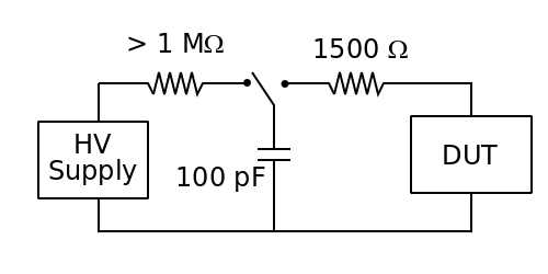
Figure 1 Simplified HBM circuit from Blog on the basic HBM waveform
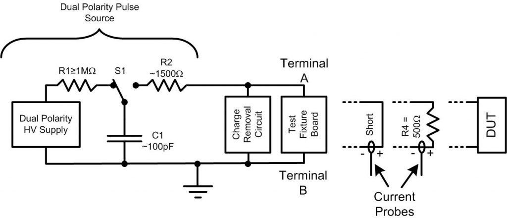
Figure 2 Reproduction of the basic circuit diagram for the HBM ESD test from JS-001
The charge removal circuit has been in various HBM standards for many years. The JEDEC HBM standard, JESD22-A114, and the military HBM standard, MIL-STD-883 Test Method 3015 included a simple switch in parallel with the device under test (DUT). The ESDA HBM standard, ANSI/ESD STM5.1, included the switch but required the switch be in series with at least a 10 kΩ resistor. The purpose of this circuit was to remove any remaining charge on the device being tested and on the test fixture before the next pulse. The switch was to be closed after the HBM pulse and then opened again before the next pulse. The resistor required in the ESDA standard was to limit current while removing residual charge. It is likely that equipment suppliers always included a current limiting resistor in the charge removal circuit as part of good system design.
The need for some form of charge removal circuit employed during the HBM pulse began to emerge with the presentation of two papers during the same session at the 2004 EOS/ESD Symposium. One involved a low level, but long-lived, current which occurred after the HBM pulse and the second involved voltages which appeared across the DUT before the HBM pulse.
In the first paper [1] it was found that after the main HBM current pulse there was a “Trailing Pulse” which lasted up to 700 us. The current is shown conceptually in Figure 3. To understand the features in Figure 3 it is necessary to know that a real relay has properties that differ from an ideal, fully off versus fully on switch. HBM testers frequently use high pressure gas mercury whetted relays. When such a relay is activated at high voltage the initial conductivity is not when the relay contacts actually touch, but when an arc forms between the relay contacts. The main HBM pulse is totally carried by this arc. Only 10s of us later do the relay’s contacts make physical contact, resulting in a second, but smaller HBM pulse. This secondary pulse has long been known and JS-001 requires that its peak current be less than 15% of the main HBM pulse. What the paper by Meuse et.al found was a long trailing current pulse of almost constant magnitude which lasted for 700 us and could be 100s of uA in magnitude.
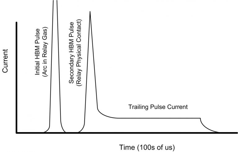
Figure 3 Conceptional representation of the current showing the main HBM pulse, secondary HBM pulse and the trailing pulse
The source of this current is the result of another artifact of a gas filled relay. After the arc which carried the initial HBM current pulse the gas in the relay remains ionized for 100s of us. The ionized gas provides a current path to the device under test all the way back to the high voltage power supply.
The trailing current could charge up the input on the DUT all the way up to the breakdown voltage of the protection diodes. The result was a sustained voltage on the input gate oxides, which resulted in a shift in transistor threshold which put input high and input low values out of specification. The result was a false HBM failure. The failure was a false failure because it was not caused by the HBM pulse itself but by the trailing pulse current which would not be present in a real world HBM event.
There are two ways to fix the issue with trailing pulses, and these are both shown in Figure 4. The more elegant is to place an extra relay, S2, between the >1 MΩ resistor and the 100 pF capacitor. Relay S2 would be closed during the charging of the 100 pF capacitor. S2 would then be opened before relay S1 is switched to initiate the HBM pulse. Since S2 is opened when the potential on each side of the relay is the same there is no arc and therefore no ionization in the relay. The DUT is therefore effectively isolated from the high voltage supply and there will be no trailing current. This is, however, a major hardware change and is not always practical.
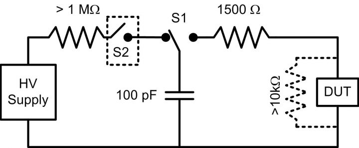
Figure 4 Fixes for the trailing pulse current issue
An easier method is to place a 10 kΩ or greater resistor in parallel with the DUT during, not just after, the HBM pulse. If the charge removal circuit in Figure 2 is a resistor adding the resistance during the HBM pulse is simply a software change. The 10 kΩ resistor will drain charge off of the DUT during any trailing pulse, preventing voltage from building up across the DUT.
The second paper [2] which led to the adoption of the 10 kΩ resistor for charge removal during HBM testing concerned voltages across the DUT before the HBM pulse. Dynamic power supply clamps were found to be failing if the power rail being tested had low capacitance and low leakage. An example of a dynamic power supply clamp is shown in Figure 5. During normal operation the inverter chain and RC network keep the large nMOS (BigFET) device off. During handling and HBM testing power is not applied so the VDD to VSS voltage is assumed to be zero. A positive ESD event on VDD will rapidly increase the potential on VDD with respect to VSS. The RC network will tend to hold the input to the first stage of the inverter chain low for an RC time constant. The inverter chain will therefore hold the gate of the large nMOS device high. With the gate high the large nMOS device will provide a non-damaging current path for the HBM stress.
Figure 5 Sample dynamic power supply clamp.
Figure 6 Voltage across dynamic clamp if capacitance and leakage were low during HBM testing. The HBM stress occurred at time = 0.
Experiments with vacuum relays [3], which do not leak due to gas conductivity, showed that the pre HBM pulse voltage was due to the varying capacitance as the relay closed, but before the arc formed to create the HBM event. The mechanism can be understood with the aid of Figure 7. The figure consists of the 100 pF capacitor in the HBM model, the capacitance across the relay, represented by a variable capacitor and the DUT, represented by a Zener diode which has its own parasitic capacitance in addition to tester capacitance. Before the HBM test system starts an HBM test event the 100 pF capacitor is charged to the HBM test voltage, for example, 1000 V. With 1000 V across the 100 pF capacitor the voltages across the relay capacitance and the DUT capacitance must be 1000 V. It is assumed that the relay capacitance is much lower than the DUT capacitance so that most of the voltage is dropped across the relay. Additionally, any leakage, RDUT, in the DUT will tend to maintain low voltage across the DUT during the relatively long charging time of the 100 pF capacitor. The situation changes when the relay begins to close to initiate an HBM test pulse. As the relay closes and the relay contacts get closer together the relay capacitance increases with a time scale of 10s to 100s of us. As the relay capacitance increases more charge is needed in the relay to maintain the voltage across the relay since V =qC. On the 100 pF side of the relay the charge must come from the 100 pF, slightly reducing the voltage across the 100 pF capacitor. On the DUT side the charge must come from the DUT. If the DUT resistance is very high (low leakage) the DUT capacitance will become charged and the voltage across the DUT will rise, as was shown in [3]. The lower the DUT capacitance and the lower the DUT leakage the larger the voltage rise will be.
Figure 7 Capacitance model to explain pre-pulse voltage
The next question on the pre-pulse voltage is; should this effect be removed from the tester because it doesn’t represent real life or is there a pre-pulse voltage during a real HBM event and ESD protection structures must be designed to protect even when a pre-pulse voltage is present. A 2006 EOS/ESD Symposium paper addressed this issue [4]. This investigation suggested that the pre-pulse voltage was an effect that can occur in a real life ESD event, but its magnitude will likely be much smaller in a real-world event. The approach speed of the contacts in a relay will likely be orders of magnitude faster than a person is likely to be able to duplicate while handling integrated circuits. The conclusion was that it was reasonable to remove or reduce the pre-pulse voltage in an HBM test system.
The most effective way to ensure that voltage does not build up across the device is to add a resistance which is low enough to maintain zero voltage across the DUT but high enough not to adversely affect the HBM pulse properties. A 10 kΩ resistor has been deemed to be a reasonable choice.
To demonstrate how much the presence of a 10 kΩ shunt resistor changes the HBM stress current SPICE simulations were made of the current through hypothetical DUT. The DUT was represented by a diode with a 100 V reverse breakdown and a 100 Ω resistance above reverse breakdown. The results are shown in Figure 8. This is a particularly bad ESD protection scheme, but shows how little the addition of the 10 kΩ shunt degrades stress on the device under test.
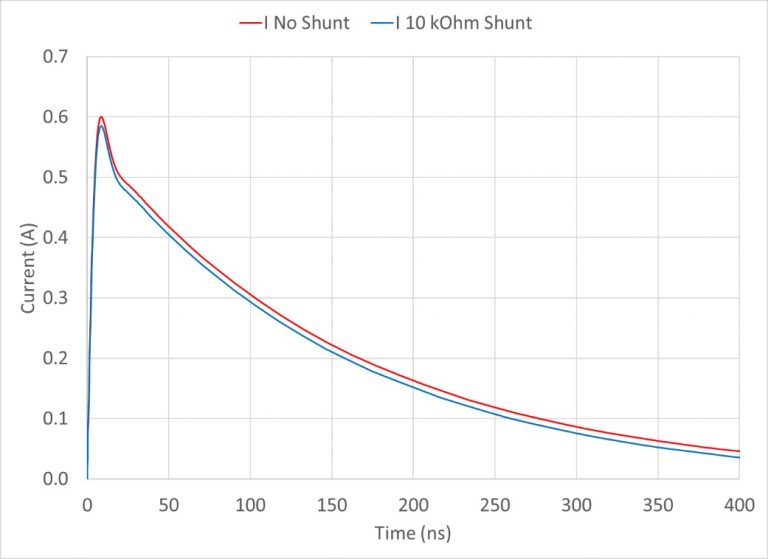
Figure 8 Comparison of HBM current through a diode with 100 V reverse breakdown and 100 Ohm dynamic resistance above breakdown with and without a 10 kOhm shunt resistor
In summary, a 10 kΩ resistor across the device under test during HBM testing can remove unwanted stress after the HBM pulse from trailing pulse current but will remove pre-pulse voltage which can prevent some types of dynamic clamps from functioning properly. This is accomplished with minimal effect on the HBM stress current.
[1] T. Meuse et.al, “Formation and Suppression of a Newly Discovered Secondary EOS Event in HBM Test Systems”, 2004 EOS/ESD Symposium.
[2] R. Ashton, B. Weir, G. Weiss, and T. Meuse, “Voltages Before and After HBM Stress and Their Effect on Dynamically Triggered Power Supply Clamps”, 2004 EOS/ESD Symposium.
[3] J. Barth, R. Ashton, E. Worley, and J. Richner, “Voltages Before and After Current in HBM Testers and Real HBM”, 2005 EOS/ESD Symposium.
[4] R. Ashton and E. Worley, “Pre Pulse Voltage in the Human Body Model”, 2006 EOS/ESD Symposium.
JULY 20, 2018 BY ROBERT ASHTON and STEPHEN FAIRBANKS
In a previous blog, HBM Basic Waveform, we discussed the circuit diagram and basic waveform for the Human Body Model (HBM) ESD stress test. That blog did not, however, address how the HBM waveform is applied to an integrated circuit. The device under test (DUT) was simply represented as a 2 pin device. One possibility would be to stress between all possible two pin combinations. This can lead to a very large number of stresses, even for low pin count devices. The number of pin combinations for a device with N pins can be written as:
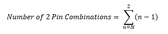
This sequence builds rather quickly. For a 10 pin device there are 55 pin combinations, for 100 pins 5050 and for 1000 pins 499,500 combinations. These numbers must be doubled to allow for positive and negative stress. It was clear to the developers of the standard that a more economical choice of pin combinations was needed.
The origin of the pin combinations in the HBM standard is somewhat shrouded in mystery. One story I have heard is that during an early HBM standards meeting a design engineer stood up and drew a simplified circuit diagram of an integrated circuit and drew the possible current paths during an ESD event. The proposal was adopted and the design engineer has not been seen since and no one knows his name. The proposal worked well for many years, although recently some modifications have been made. In this blog post I will introduce the traditional HBM pin combinations which are in Table 2B of the Joint JEDEC/ESDA HBM standard JS-001 2017 [1]. In a later blog I will address Table 2A with the newer pin combinations and the motivations for the updates as well as how testing can be done with a 2 pin tester.
Table 1 is a reproduction of Table 2B in JS-001-2017 and is the traditional set of pin combinations which have been used for many years in the joint JEDEC/ESDA HBM standard JS-001 2017 and the separate JEDEC and ESDA HBM standards which proceeded JS-001. To understand the pin combinations, it is necessary to understand three terms, supply pin, supply pin group and non-supply pin. JS-001 goes into a great deal of detail on these terms, but in this blog we will focus on the basics needed for understanding pin combinations.
A supply pin is any integrated circuit pin used to provide power to the circuit. It is important to know that ground pins are considered power pins. Typical names for supply pins are, VDD, VDDA, VSS, VSSA, GND and as well as many variations on these names.
The power demands for many integrated circuits (IC) are large enough that a single pin cannot supply all of the current needed by the device without excessive voltage drops and power dissipation, either within the IC or in the connection of the IC to a printed circuit board. In these situations, from 2 to dozens of supply pins may be tied together with metal on the die of the IC or in the package. Supply pins tied together in this manner create a supply pin group. Note that even though two supply pins may have the same supply voltage they are not part of the same supply pin group unless they are metallically connected on the die or in the package. For example, a digital ground and an analog ground may both be tied to ground on a circuit board, but they are not part of the same supply pin group because they are likely isolated from each other on the die of the IC. We will see an example of this when we give examples in the next section. (JS-001 has additional requirements of low resistance between pins within a supply pin group as well as conditions in which a single pin can represent a supply pin group, but for simplicity we will not address those conditions here.)
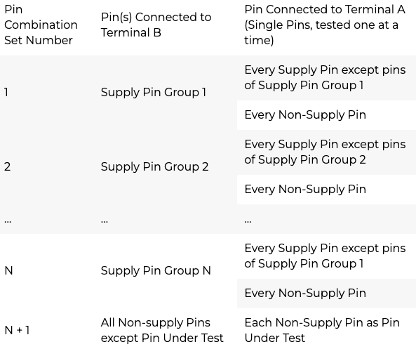
Table 1 Traditional JEDEC/ESDA pin combinations for HBM testing. This table is a copy of Table 2B in JS-001 2017
Once supply pins are understood it is easy to understand non-supply pins. Non-supply pins are simply all pins which are not supply pins or no connects. Non-supply pins are mostly inputs, outputs and input/output pins. No connect pins are package pins with no connection to the IC die. No connect pins are not tested during HBM and may be a topic for a future blog post.
Table 1 shows there to be N + 1 sets of pin combinations, where is N is the number of supply pin groups. In the n = 1 to N sets of pin combinations each of the supply pin groups are shorted together and connected to the B terminal of the HBM tester. (The B terminal of an HBM tester is the side closer to ground, while the A side is connected to the HBM pulse source. The B side of the HBM tester is not strictly ground since termination resistance is needed to suppress reflections.) While all pins of supply group n are connected to terminal B, each supply pin not part of supply pin group n is connected to terminal A, one at a time, and positive and negative HBM stress is applied from terminal A to terminal B. This is repeated for each of the N supply pin groups.
After all supply groups 1 to N have been connected to terminal B, non-supply to non-supply stress needs to be addressed. To reduce test time and number of stresses the early HBM standards groups elected not to stress each non-supply pin to every other non-supply pin individually. Instead each non-supply pin was connected to terminal A, one at a time, and stressed versus all other non-supply pins shorted together and connected to terminal B. This arrangement is not exactly realistic but does save considerable test time.
In this section we will show how the pin combinations above test out the ESD protection on a popular style of ESD protection, which uses steering diodes on all inputs and outputs coupled with ESD protection circuits between all power supplies and their respective grounds. The VDD to VSS protection could be of the form of a dynamic clamp as presented in [2]. Dynamic clamps prove protection during a positive transient on VDDn versus VSSn. For a negative stress protection is provided by the diode naturally present between VDDn and VSSn. This ESD protection strategy can provide a low impedance current path for ESD stress between any two pins on the integrated circuit. How this scheme works will become clear as we discuss pin combinations.
Figure 1 shows a simple schematic which we will use to represent a full integrated circuit. It includes two power supply domains (4 supply pin groups) VDD1-VSS1 and VDD2-VSS2 as well as Inputs and Outputs for each of the power domains. The two VSS busses are isolated from each other with a pair of anti-parallel diodes to create plus and minus diode drop of isolation between the grounds. Note that each VDD and VSS supply pin group may be represented by from 1 to dozens of individual package pins.
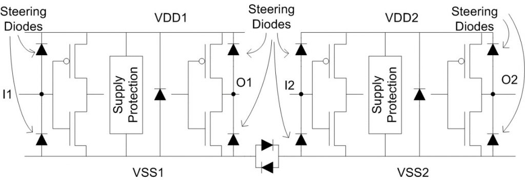
Figure 1 Representative schematic of an integrated circuit using power supply protection with steering diodes on all IOs
Figure 2 and Figure 3 illustrate positive and negative stress respectively on supplies VDD1, VDD2 and VSS1 on Terminal A versus VSS2 on Terminal B. For both the positive and negative stresses VSS1 to VSS2 the diodes between the two VSS lines provide a low impedance path between the supply domains. Positive stress to VDD pins uses the Supply Protection to provide the low impedance path during stress.
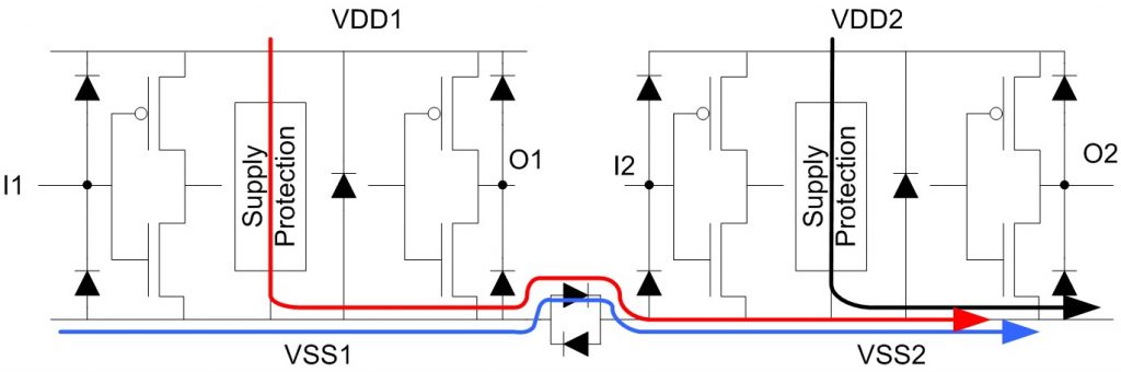
Figure 2 Positive stress from VDD1, VSS1 and VDD2 on Terminal A to VSS2 on Terminal B
During negative stress on VDD1 and VDD2 the diodes inherently present in the technology provide the low impedance paths from VDD to VSS.
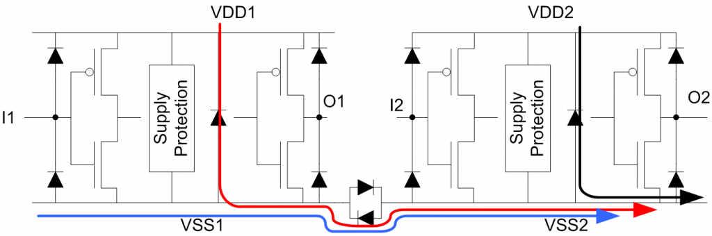
Figure 3 Negative stress from VDD1, VSS1 and VDD2 on Terminal A to VSS2 on Terminal B
Figure 4 and Figure 5 illustrate the low impedance current paths for positive and negative stress of non-supply pins respectively. Note how the steering diodes “steer” the current to the VDD and VSS lines. Once the stress is directed to the VDD and VSS lines the current paths are similar to the paths used during stress of supply pins.
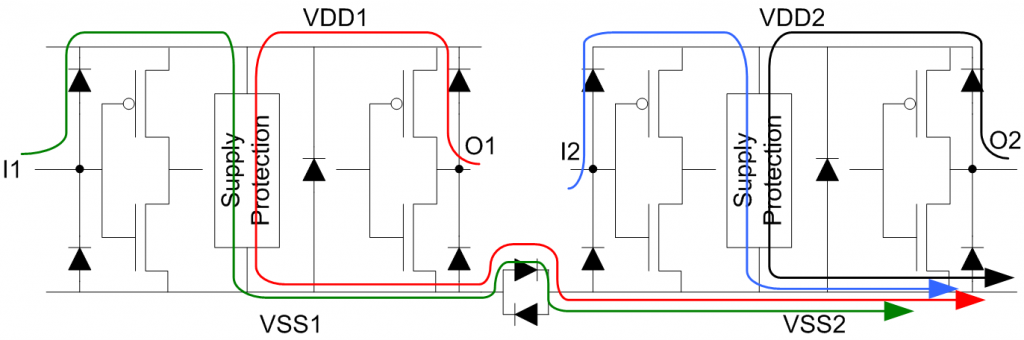
Figure 4 Positive Stress from non-supply pins on Terminal A to VSS2 on Terminal B
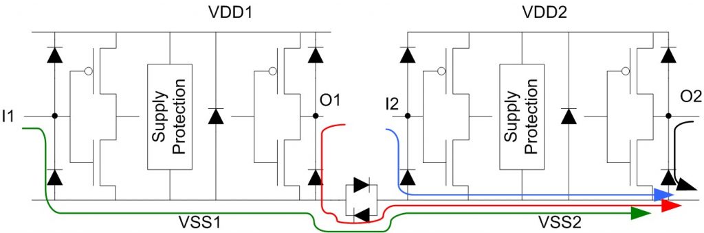
Figure 5 Negative Stress from non-supply pins on Terminal A to VSS2 on Terminal B
Pin Combinations N + 1 from Table 1 result in somewhat more complicated current paths for each stress, since all non-supply pins not connected to Terminal A are tied together in the tester to Terminal B. The possible current paths for the stress of I1 versus all other non-supply pins are shown in Figure 6 and Figure 7 for positive and negative stress respectively. If we follow the current paths for I1 to other non-supply pins in Figure 6 or Figure 7 we see that the current path that leads to the other non-supply pin in the VDD1-VSS1 power domain has one fewer forward bias diode drops than the current paths to the pins in supply domain VDD2-VSS2. It is therefore likely that most of the stress current will remain within the VDD1-VSS1 power domain.
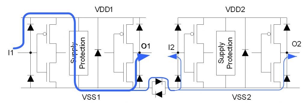
Figure 6 Positive Stress on I1 on Terminal A versus all other non-supply on Terminal B
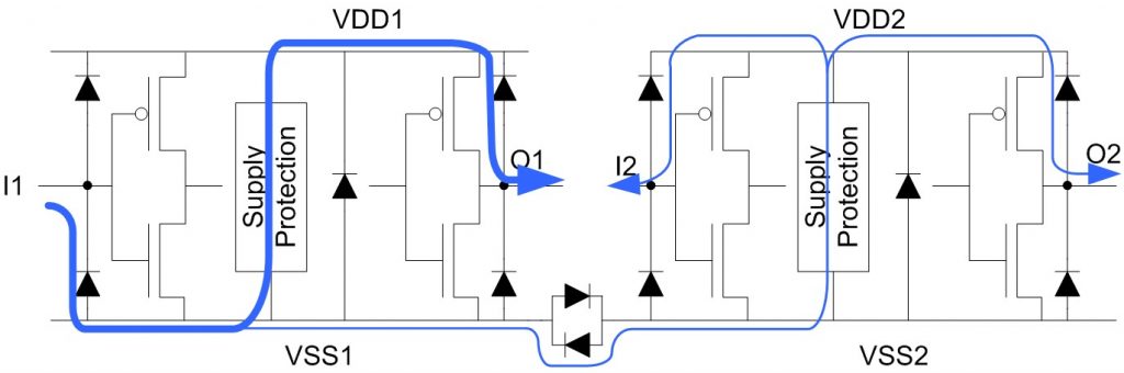
Figure 7 Negative Stress on I1 on Terminal A versus all other non-supply on Terminal B
In this article we have discussed the traditional pin combinations that have been used during HBM testing for many years. A sample circuit was used to demonstrate how the traditional pin combinations exercised all of the necessary low impedance paths which must exist for proper protection of an integrated circuit from HBM stress. These pin combinations have served the electronics industry for many years and have prevented integrated circuits with poor HBM performance from entering the marketplace.
The traditional pin combination represented in Table 1 (Table 2B in JS-001-2017) are not without issues however. As the number of supply pin groups has increased over the years from 2 to dozens on large integrated circuits the number of pin combinations has increased dramatically. The result has been excessive test times and wear out of the integrated circuit as sections of the integrated circuit are tested up to thousands of times during HBM testing. In a future article we will address how Table 2A in JS-001 2017 can reduce stress time and wear out. In another future article we will discuss how two pin testing can be performed on high pin count circuits without excessive test times using the provisions in JS-001.
DECEMBER 11, 2017 BY ROBERT ASHTON and STEPHEN FAIRBANKS
Welcome to Minotaur Labs’ new Blog on ESD testing. For each post we will discuss a particular topic related to ESD testing. In addition to describing some of the important aspects of ESD testing we will let you know about the latest developments in ESD testing standards. We hope you find these posts useful and interesting. Please let us know what you think.
For our first post we will discuss the Human Body Model (HBM) waveform. The HBM test is intended to simulate an electrostatically charged person discharging through an integrated circuit. If you look in the latest version of the joint JEDEC/ESDA HBM standard, ANSI/ESDA/JEDEC JS-001-2017 you will see a circuit diagram similar the one shown in Figure 1. A high voltage power supply charges a 100 pF capacitor and then with a flip of a switch, discharges through a 1500 W resistor into the device under test (DUT).

Figure 1 HBM Circuit
If the DUT is close to a short the circuit diagram implies the blue current versus time curve shown in Figure 2 for 2000 V. The instantaneous rise of the current to 1.33 A is of course not realistic; inductance, capacitance and the finite turn on time of the switch will round off the peak. The specifications for the actual current waveform in JS-001 into a short are given as:
An idealized waveform, compliant with these specifications, is shown in red in Figure 2. The most obvious change is the slower rise time and rounded peak to the waveform. The 2 ns to 10 ns rise time is obviously a very wide window, but there are practical reasons for this. Delivering a fast-rising current pulse to an integrated circuit is not an easy task, and the wide range of rise times gives test equipment designers a reasonable tolerance range for equipment design. In fact, most HBM test systems have rise times nearer to the high side of the specification than the low end of the specification.
There are some subtleties to how these specifications are applied to a measured waveform, as well as criteria for a 500 W load in addition to the short, but those are topics for another post.
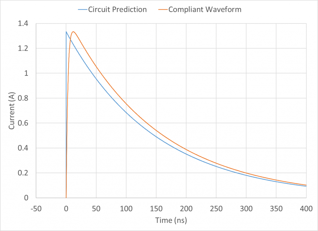
Figure 2HBM waveforms for 2000 V
The question that is often raised; is this waveform realistic for a real HBM event on a factory floor and if not, what should the waveform be? The original waveform captures used to establish the HBM event are certainly not as good as the ones made by Jon Barth and his co-authors in 2003 [1]. They measured discharges from people charged to various voltages and measured the discharge current under very controlled conditions with a 6 GHz oscilloscope and a high bandwidth current sensor. A sample waveform is shown in Figure 3. At first glance this real waveform is similar to the standardized waveform. There is a rapid rise in current, followed by a slower decay. Looking into the details, the Barth team found significant difference between the standard waveform and real world HBM. In a dry atmosphere they found very fast rise times, an order of magnitude faster than the 2 ns to 10 ns risetime specification. The results were also very dependent on humidity, high humidity reduced peak heights and increased the rise time. Geometry also affected the results, flat surfaces created the fastest rise times and higher peak currents, while a pointed discharge surface also reduced peak heights and increased rise times. The current decay also differed from a pure exponential decay. The decay started out with a decay faster than the standard 150 ns time constant, but then the discharge rate slowed as the discharge progressed. These effects are all related to the properties of an arc forming in air. This is a very complex physical process and some of the details are discussed in the Barth paper.
DECEMBER 11, 2017 BY ROBERT ASHTON and STEPHEN FAIRBANKS
In a previous blog I discussed the basics of the Human Body Model (HBM) current waveform. The simplified circuit is shown in Figure 1. As discussed in the previous blog, for a low impedance device under test (DUT) this produces a fast-rising current pulse with an approximately 150 ns exponential decay time. Of course, real HBM test systems are much more complex than shown in Figure 1. For testing high pin count integrated circuits matrix based HBM test systems are often used. These systems provide a convenient automated testing of complex integrated circuits. Unfortunately, complex systems can have unexpected consequences. In this blog I will discuss how parasitics introduced by the relay matrix can have negative impact on the stress waveform, which can lead to false failures.
Figure 1 HBM Circuit
Figure 2 shows a conceptual schematic of a matrix based HBM test system. A relay matrix allows any single pin to be connected to the HBM pulse source and one or more pins to be connected to ground. The matrix based HBM tester opened the way for fully automated HBM testing, allowing the many HBM pin combinations to be performed rapidly and with confidence. In 2004, however, a paper was presented by Texas Instruments (TI) [1] which showed that parasitics in the switch matrix could distort the stress applied to the DUT and lead to false failures. The ESDA HBM standards working group did further work to understand tester parasitics and published a paper in 2006 elaborating the issue [2].
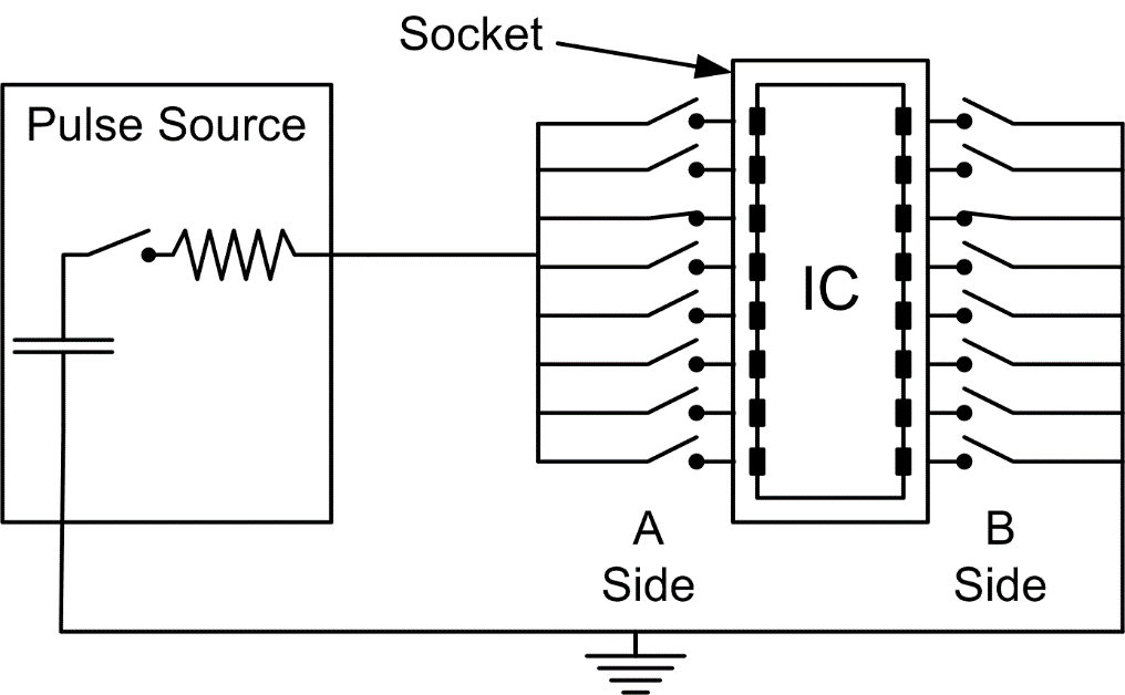
Parasitic capacitance and inductance are present in all electronic systems. The HBM specification recognizes the presence of parasitics by having a fairly wide rise time specification as well as placing an upper limit on parasitic capacitance by requiring a 500 ohm qualification test which will expose extensive parasitic capacitance. The TI paper showed that when an integrated circuit (IC) is inserted into the tester’s socket the IC can interact with the tester to distort the waveforms the DUT sees. The problem is illustrated in Figure 3, where three channels of the HBM tester have been shorted together by the IC. The short is usually due to power supply domains which have multiple pins. The potential for shorting several pins together is straight forward when stressing one pin on a power supply domain with many pins. It can also happen when an I/O, which includes didoes to power and ground, is stressed. During the stress the diodes become forward biased, essentially connecting the stressed IO to a power supply domain. While these parallel capacitive current paths can’t carry a dc current, they can carry current during a transient. This will modify the current through the intended path in the IC.
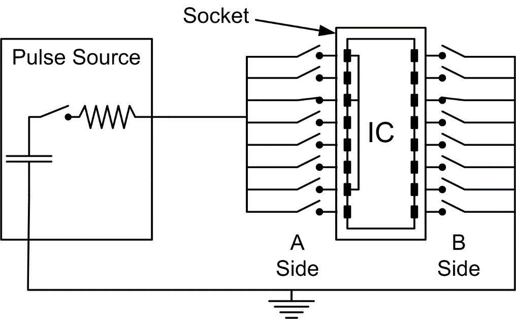
Figure 3 Schematic of Matrix HBM tester showing how internal connections in an integrated circuit can tie tester channels together
This can be seen more clearly in the schematic in Figure 4. The schematic for the HBM pulse source is based on the schematic proposed by van Roozendaal and his coauthors in 1990 [3], and uses values of inductance and capacitance in parallel with the main HBM resistor based on value extracted by Verhaege and his coauthors [4]. The 6 uH inductor provides the slow, several ns, rise time for the HBM waveform, while the 1.5 pF capacitor results in the slight overshoot in the waveform which will be seen below. In the simulations the DUT resistance will be assumed to be zero because during an ESD event ESD protection elements in most ICs will have resistances of just a few ohms. This is much less than the 1500 ohm source resistance of the HBM pulse source.
One of the first questions that might be asked about the diagram in Figure 4 is why is there a 50 ohm resistor in the DUT channel of the tester? That doesn’t match the circuit diagram in Figure 1. The answer is that without some form of termination resistor on the ground side of the DUT there would be very large reflections in the system. Reference [2] found that the termination values on different matrix based tester varied from 50 to 100 ohms.
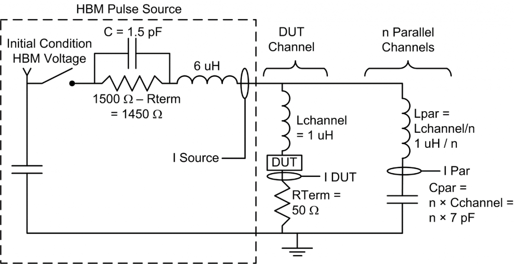
Figure 4 Schematic used in simulations
Before discussing the simulation results it is important to note that these simulations are for example only. They do not represent any specific tester, although the general trends match some of the measurements reported in [2]. It is also important also to note that the simulations are a lumped element model and may not accurately represent the distributed elements present in a real HBM test system.
Simulation of the current as measured at the HBM Source (I Source) is shown in Figure 5 with from no parallel parasitics to 32 channels of parasitics. The added parasitic elements result in extra ringing, but little change to the overall waveform. The situation changes dramatically if we look at the current measured through the DUT, as shown in Figure 6. The parallel channels create extensive ringing in the current through the DUT. The cause of this ringing can be seen more easily if we compare the HBM source current, DUT current and Parasitic path current for a particular number of parasitic channels. This is shown in Figure 7 for the case of 32 parallel parasitic paths.
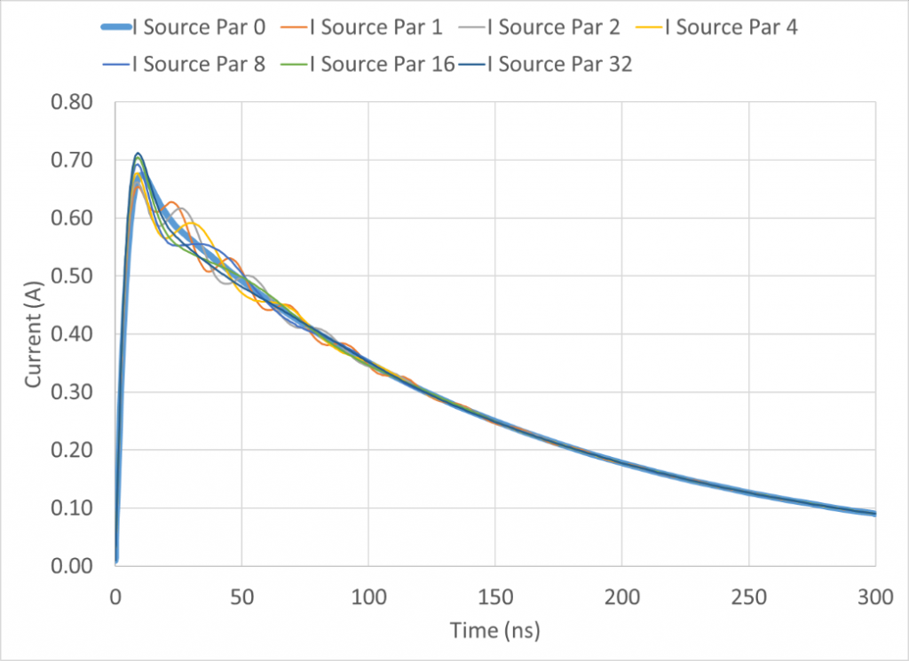
Figure 5 Simulation of HBM Source Current with 0 to 32 parasitic channels in parallel to the DUT channel
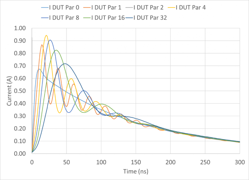
Figure 6 Simulation of Current through the DUT with 0 to 32 parasitic channels in parallel to the DUT
It the beginning of the HBM pulse the capacitance of the parasitic path provides a lower impedance than the DUT in series with the termination resistor. Significant current doesn’t start to flow in the DUT until the parasitic capacitance becomes charged and the DUT becomes the preferred current path. With the capacitor charged the circuit loop consisting of the DUT, termination resistor, channel inductances and parasitic capacitor acts as a classic underdamped LCR resonant circuit.
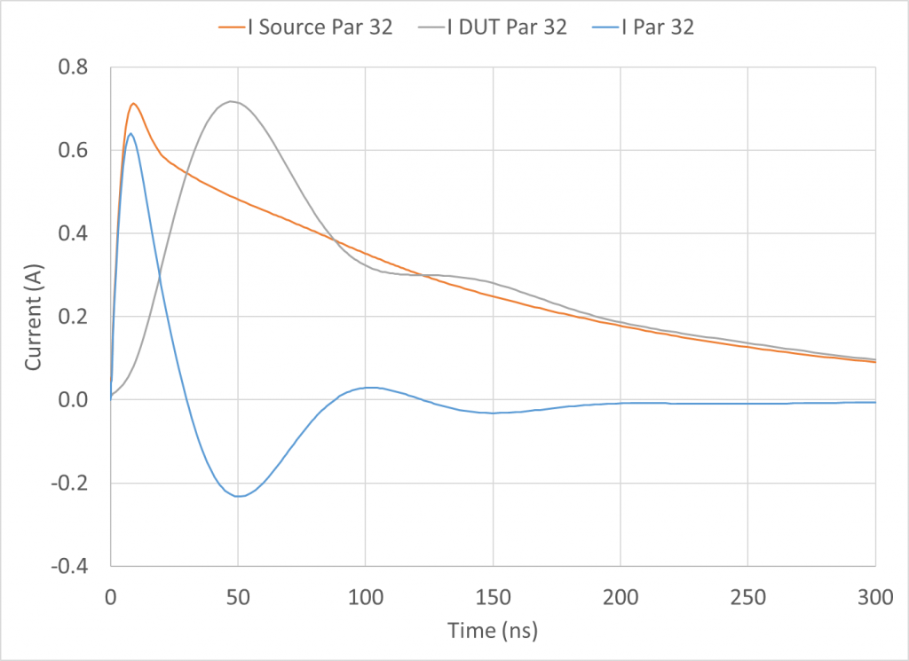
Figure 6 Simulation of Current through the DUT with 0 to 32 Figure 7 The current in the HBM Pulse Source, through the DUT and in the Parasitic Channels for the case of 32 parallel parasitic channels channels in parallel to the DUT
The important question is, how does this affect test results. A number of papers such as [1] have reported issues with false failures due to tester parasitics. Some protection design styles may not be sensitive to parasitcs, but dynamic circuits sensitive to stress rise times could be very sensitive.
What can be done to reduce the effects of tester parasitics? Thermo Fisher has introduced an ultra-low parasitic version of their Mk2 which reduces each channel’s capacitance by an order of magnitude. Another option is the two pin HBM system from Grund Technical Solutions which uses wafer probe needles to stress packaged devices with HBM. This virtually eliminates parasitics during HBM testing. I will discuss this type of testing in a future blog post.
References
[1] Kunz et al., “The Effect of High Pin-Count ESD Tester Parasitics on Transiently Triggered ESD Clamps”, EOS/ESD Symposium, 2004.
[2] Chaine et al., “HBM Tester Parasitic Effects on High Pin Count Devices with Multiple Power and Ground Pins”, EOS/ESD Symposium, 2006.
[3] van Roozendaal et al., “Standard ESD Testing of integrated Circuits,” EOS/ESD Symposium, 1990.
[4] Verhaege et al., Analysis of HBM ESD Testers and Specifications Usijng a 4th Order Lumped Element Model”, EOS/ESD Symposium, 1993.
created with
Website Builder Software .